


Nomenclature
Subscript
1. Introduction
2. Hole Transport Layer (HTL)
2.1 Inorganic HTLs
2.2 Organic HTLs
3. Interfacial Layers
3.1 Inorganic HTL-Based Solar Cells
3.2 Organic HTL-Based Solar Cells
4. Conclusions
Nomenclature
PCE : power conversion efficiency, %
VOC : open circuit voltage, V
FF : fill factor, %
JSC : short circuit current density, mA/cm2
Subscript
PV : photovoltaics
TF : thin-film
Sb2(S,Se)3 : antimony sulfoselenide
ETL : electron transport layer
HTL : hole transport layer
CuSCN : copper(I) thiocyanate
P3HT : poly(3-hexylthiophene-2,5-diyl)
KPFM : Kelvin Probe Force Microscopy
SCLC : Space charge limited current
XRD : X-ray diffractometry
UPS : ultraviolet photoelectron spectroscopy
HRTEM : high resolution transmission electron microscopy
SEM : scanning electron microscopy
IZO : amorphous indium-zinc oxide
TCO : transparent conducting oxide
VS : sulfur vacancy
ITO : indium tin oxide
WF : work function
QFLS : quasi Fermi level splitting
1. Introduction
Various renewable energy sources have been developed to counter adverse environmental effects of fossil fuels, and solar energy distinguishes itself from the rest with its virtually inexhaustible energy source in the Sun and freedom from harmful emissions. Furthermore, excellent scalability enables versatile applications to both small and large-scale needs1). Solar PV involves generation of electrical energy from sunlight via exploitation of the photoelectric effect in semiconducting materials, and silicon has been at the forefront of innovation and commercialization of this technology2). Si solar cells are classified as a first-generation PV cell, but they are still relevant and dominant in the PV field, as evidenced by high efficiencies and global market share of around 90%3). Despite the relevance, Si solar cells are hindered by their brittle and rigid properties that limit their applications on flexible substrates in addition to their relatively high processing temperatures4). Also, achievement of high efficiencies entails high production costs for pure, defect-free silicon5). TF solar cells have been actively studied to produce cells that possess flexibility and involve lower material consumption and production costs. The main merit of TF solar cells would be absorbing amount of solar energy like the one obtained through Si solar cells by covering a transparent substrate with a thin layer of photoactive absorber material, ultimately achieving similar efficiencies with a single processing step and material consumption amount reduced by 99%6). CIGS, CdTe, and perovskites are some of the most prominent types of thin-film PV cells. Unfortunately, these cells suffer from respective major disadvantages that diminish their upsides. CdTe has lower production costs compared to crystalline Si and is appropriate for flexible applications, but the toxicity of Cd and scarcity of Te limits its potential7). CIGS yields high efficiencies in low-light environments, but the toxicity of Se paired with scarcity of In and Ga poses unfavorable conditions8). Although perovskites offer benefits in low production costs, tunable direct band gaps, potential for high efficiencies due to its ability to absorb light in the visible spectrum, and solution processing method that does not require high temperatures like in production of Si cells, the cons are as undeniable as the pros, including toxicity of lead content, limited flexibility, and stability (which is heavily affected by humidity, UV light, and thermal stress)9). Sb2(S,Se)3 emerged as a suitable absorber material that can differentiate itself from the aforementioned materials with its earth-abundant composition, tunable band gap (1.1-1.7eV), high absorption coefficient, unique quasi-1D microstructure, stability in air and moisture, and non-toxicity10). A typical structure of Sb2(S,Se)3 solar cells involves a superstrate structure, where light enters from the supporting glass substrate; the components are constructed in the order of transparent conductive oxide glass/ETL/Sb2(S,Se)3 light absorber layer/HTL/electrode back contact11). However, the PCE values are significantly below the theoretical Shockley-Queisser limit, and interfacial engineering is one of the key facets in the improvement of PCE values12). HTL material choice is a crucial factor because the unique quasi-1D structure of Sb2(S,Se)3 could result in poor interface energetics with certain HTLs like Spiro-OMeTAD characterized by poor valence band alignment and stability13). Therefore, both inorganic (i.e. NiOx MoO3 and MnS) and organic (i.e. phthalocyanine) materials have been explored to identify and broaden the list of compatible HTLs14, 15, 16, 19, 20, 21). Back contact engineering is also an essential facet to consider, for fill factor and VOC are directly influenced by interfacial band alignment and recombination. Interlayer buffer layers like trigonal selenium (t-Se) are being developed to enhance selective charge extraction, stability, and defect passivation through optimization of surface composition and band bending17). The aim of this paper is to introduce some of the recent noteworthy progress in interfacial engineering of Sb2(S,Se)3 solar cells achieved particularly through HTL material and buffer/interlayer engineering. Recent certified efficiency benchmarks and performance trends across photovoltaic technologies are summarized in the Solar Cell Efficiency Tables35). For Sb2Se3 in particular, defect- and trap-limited analyses suggest substantial rooms for improvement beyond the current efficiency plateau36).
2. Hole Transport Layer (HTL)
HTLs function to facilitate hole transport and block electrons at the back interface for improved band alignment and prevention of leakage current. Like ETLs, significant efforts are being made to implement novel HTL materials and structures for improvement of solar cell parameters. Organic materials, including Spiro-OMeTAD and P3HT, have been prominently used as HTLs, but they are subject to bottlenecks such as chemical and thermal instability, expensive costs, and complex synthesis processes that prevent further innovation. Therefore, replacing these organic HTLs with inorganic materials alternatives that offer lower costs, superior chemical and thermal stability, and good hole mobility has been an intensely researched facet of interfacial engineering. In Sb2Se3 and Sb2(S,Se)3 devices, the HTL/back-contact region strongly affects band alignment, hole extraction, and interfacial recombination; recent PCE values exceeding 10% for Sb2Se3 devices highlight the importance of simultaneously optimizing absorber quality and interface/HTL design37, 38).
2.1 Inorganic HTLs
Compared with organic HTLs, inorganic HTLs offer superior thermal and chemical stability and are therefore attractive for Sb2(S,Se)3-family devices, where the back contact is prone to forming a non-ohmic barrier because of the relatively low intrinsic carrier density of the absorber. Notably, certified device efficiencies have advanced rapidly through absorber and junction/interface engineering (e.g., a 7.6% certified CdS/Sb2Se3 device via vapor transport deposition and a 9.2% certified nanorod-array architecture via junction interface engineering), underscoring the importance of simultaneously optimizing hole-selective back contacts40, 48). In addition to hole extraction, inorganic HTLs can passivate the buried back surface, tune band bending, and suppress detrimental interfacial reactions (e.g., Au diffusion), thereby improving both VOC and fill factor31, 32, 33). Even when the absorber quality is substantially improved (e.g., solvent-assisted hydrothermal deposition enabling >10% class Sb2(S,Se)3 devices), back-contact losses remain a key efficiency limiter, motivating continued development of robust inorganic HTLs and interlayers34). CuSCN is a prototypical inorganic, wide-bandgap p-type semiconductor HTL that can be processed at low temperature. In n–i–p Sb2Se3 devices, Li et al. showed that CuSCN reduces back-surface recombination and increases built-in potential, enabling 7.50% efficiency25). Similar motivations have driven the adoption of CuSCN in hydrothermally deposited Sb2S3 semitransparent architectures, where improved band alignment and hole selectivity helped raise VOC and PCE compared with a PEDOT:PSS control18). Beyond simple energy-level matching, CuSCN can supply Cu ions that modify local electrical properties of Sb2Se3 grain boundaries, which has been proposed to assist carrier separation25). In Sb2Se3, a representative n–i–p configuration using CuSCN as the HTL has reached 7.5% efficiency25). Beyond CuSCN, other inorganic semiconductors have been explored to combine hole selectivity with defect passivation at the back interface. A notable example is the PbS colloidal quantum dot (CQD) film used as a hole-transporting layer, which enabled a certified 6.5% efficient Sb2Se3 solar cell and highlighted the potential of nanostructured inorganic HTLs to improve both contact energetics and interfacial recombination26). For Sb2(S,Se)3, MnS has emerged as a robust all-inorganic HTL/back-contact layer: Wang et al. reported efficient and stable Sb2(S,Se)3 devices using MnS to replace Spiro-OMeTAD, demonstrating that wide-bandgap sulfides can address stability and cost constraints while maintaining competitive performance14). In a later study, Qian et al. leveraged MnS/ITO back contacts to realize bifacial and semitransparent Sb2(S,Se)3 devices suitable for single-junction and tandem-relevant architectures29). Alternative chalcogenide HTLs such as CuSbSe2 and CZTS have also been explored to reduce lattice mismatch and mitigate back-interface recombination45,46). Transition-metal oxides (TMOs) constitute another major class of inorganic HTLs due to their high work function, transparency, and compatibility with vacuum or solution processing. V2O5 has been demonstrated as a hole-transporting material for planar all-inorganic Sb2S3 devices, where post-annealing was critical to balance interfacial cleanliness with work-function tuning and contact resistance27). NiOx is particularly appealing because it can be deposited by scalable chemical routes; for Sb2(S,Se)3, spin-coated NiOx has been used to mitigate back-contact recombination and improve device efficiency28). However, the relatively low conductivity of many TMOs means that thickness optimization, defect control, and (when chemically compatible) doping are typically required to prevent series-resistance penalties. For example, solution-processed NiOx has improved both average efficiency and device stability in Sb2Se3 cells44), while evaporated MnS has enabled stable all-inorganic Sb2(S,Se)3 devices with favorable valence-band alignment50). Notably, several back-contact “interface engineering” strategies act similarly to inorganic HTLs by inserting ultrathin inorganic interlayers that modify energetics and passivate defects at the back contact. In flexible Sb2Se3 devices, the introduction of a PbSe interlayer at the buried back-contact interface has been reported to synergistically improve back-contact selectivity and bulk transport, enabling high-efficiency flexible cells30). Similarly, ultrathin wide-bandgap oxides such as SnOx can suppress interfacial recombination while maintaining tunneling-enabled transport across the back contact24). Overall, the inorganic-HTL overlaps strongly with general back-contact interface engineering, and future progress will likely come from designing chemically benign, diffusion-stable layers that provide both field-effect passivation and low-resistance hole extraction.
2.2 Organic HTLs
Organic HTLs are attractive for Sb2Se3/Sb2(S,Se)3 photovoltaics because their energetics and surface chemistry can be tuned (e.g., polymers, small molecules, and quantum-dot layers) to improve valence-band alignment and suppress back-interface recombination. In Sb2Se3 n–i–p devices, PbS colloidal quantum dot HTLs and polymeric HTLs (e.g., P3HT) have been shown to enhance hole selectivity and mitigate shunt/pinhole-related leakage at the back contact40, 39). More recently, a dithieno[3,2-b:2′,3′-d]pyrrole (DTP)-cored molecular HTM enabled 9.7% Sb2(S,Se)3 devices, underscoring the potential of high-mobility small-molecule HTMs beyond conventional Spiro-OMeTAD49). However, the stability and cost challenges of doped organic HTMs continue to motivate inorganic substitutes in fully inorganic device stacks50). Five triazatruxene HTL variants in solar cell devices with the structure of FTO/CdS/Sb2(S,Se)3/HTL/Au were examined with SCAPS-1D by analyzing effects of variations in ETL and HTL thickness, acceptor density (NA), donor density (ND), and absorber thickness. The simulations resulted in efficiency values of 23.09%, 22.47%, 21.08%, 23.24%, and 23.11% for solar cells based on triazatruxene variants. Tangible increases in VOC, FF, and JSC were also achieved through optimization of the band alignment and QFLS. The significance of this work lies in the integration and active utilization of simulation technology with laboratory work unlike conventional laboratory work involving just physical, experimental procedures.
3. Interfacial Layers
Aside from expansion of HTL material choices from conventional organic materials to relatively new ones in inorganic, wide band gap materials, research is being carried out to develop buffer/interfacial layers for enhancement of HTL performance. Beyond the choice of HTL itself, dedicated back-contact and interfacial modification strategies have been widely used to reduce contact barriers and suppress non-radiative recombination. Examples include chemical/ambient treatments that improve the Sb2Se3 back contact42), intentional insertion layers that tune band bending and contact energetics41), and intermediate layers (e.g., MoO2) that reduce deleterious interfacial reactions while improving hole transport at the metal/absorber interface47). These concepts are also compatible with lower-cost electrodes (e.g., carbon) when combined with appropriate interface control43).
3.1 Inorganic HTL-Based Solar Cells
Yang et al. implemented a dual-function IZO layer into a solar cell with structure of FTO/CdS/Sb2(S,Se)3/MnS/IZO/ITO for protection of underlying MnS HTL during TCO electrode deposition; sulfur loss is probable due to its high saturation vapor pressure, and tendency of MnS to crystallize only aggravates this situation, making the IZO layer an essential component. With minimized sulfur loss, VS are reduced, contributing to a champion PCE value of 8.26% due to enhanced hole extraction22). Other than its protective role, the IZO layer facilitates efficient hole transport and improvement in interface contact; Schottky contacts with high energy barriers due to large discrepancies in work functions of ITO and MnS are reduced, and the downward band bending at the MnS/ITO interface that impedes carrier transport is effectively prevented. From a photovoltaic standpoint, low VOC and FF stemming from non-ohmic Schottky contacts leading to unfavorable back interface are the main causes behind a relatively low PCE (5.95%) of the reference solar cell without the IZO layer. Except for JSC, other parameters including VOC, FF, and PCE were drastically increased with the introduction of IZO layer. The integrated current density values obtained from EQE measurements were within 1% deviation from the J-V measurements, bolstering credibility. The authors further investigated back interface contact by making photovoltaic measurements for hole-only devices with respective structures of FTO/NiOx/MnS/ITO and FTO/NiOx/MnS/IZO/ITO. While the former with no IZO layer displayed asymmetric J-V characteristics that imply the formation of Schottky contacts and consequent double-sided hole barriers, the latter is characterized by a linear J-V relationship associated with ohmic contact. According to UPS, the greater WF of ITO compared to MnS will facilitate electron flow from ITO to MnS; the downward energy band bending contributes to formation of hole barriers. This phenomenon further decreases the VOC due to quasi-Fermi level splitting and drift. On the other hand, the higher WF of IZO relative to MnS enables formation of a quasi-ohmic contact interface, which enhances VOC. According to HRTEM micrographs, the discrepancies between the blurry MnS/ITO interface and the clear MnS/IZO interface imply the damaged MnS crystal structure, which is affirmed by the Fourier transform images that revealed notably defined crystalline features of ITO compared to IZO. As IZO is amorphous, XRD peaks associated with it were not present. EDS data from TEM analysis indicated that S:Mn ratio is higher for the device with IZO layer, which is consistent with the previously mentioned mechanism in which hole extraction is improved through minimization of VS and Schottky contact barriers. KPFM and AFM mappings for surface potential distributions showed that ITO and MnS, both of which are polycrystalline, have higher surface potential amplitudes compared to IZO, which means there is greater inhomogeneity on crystalline surfaces. Therefore, the relatively uniform IZO surface potential can be said to significantly enhance hole transport. The Sb2(S,Se)3 device previously discussed can be further incorporated into a 4-Terminal tandem device variant as a top cell along with a Sb2S3 bottom cell with a n-i-p structure of FTO/SnO2/CdS/Sb2Se3/Spiro-OMeTAD/Au. The top cell with an absorber of higher band gap is responsible for short-wavelength photons, while the bottom cell receives the remaining long-wavelength photons. While the respective PCEs of the top and bottom cells were 8.22% and 9.08%, a record champion PCE of 10.69% for all-Sb-based tandem device was reached. Furthermore, an attractive 20.86% PCE was observed during indoor usage of these cells, hinting at the diversity of applications that are derived from the IZO dual function layer. More broadly, recent record-efficiency Sb2Se3 devices emphasize tight control of absorber growth and carrier-selective contacts/interlayers37, 38).
3.2 Organic HTL-Based Solar Cells
Related organic-interface approaches (including molecular HTMs and organic layers that improve back-contact selectivity) have been reported for Sb2Se3/Sb2(S,Se)3 device stacks39, 49). Interfacial layers for Sb2(S,Se)3 solar cells with organic HTLs are being studied as well. Wu et al. developed and introduced two organic self-assembled monolayers (SAM) termed TPA-2Th and TPA-2Py into Sb2(S,Se)3 devices as a passivation layer inserted between the absorber and hole transport layers for photovoltaic performance enhancement through modification of the interfacial band bending profile23). Fig. 1 outlines the mechanism by which the SAM molecules alter the surface electronic structure and cause shift of the surface Fermi level and an increase in work function, ultimately making the absorber surface and band alignment more favorable for hole extraction. Fig. 2 further bolsters the impact of the SAM interlayer by showing surface potential profiles and KPFM images that indicate increases in contact potential difference and absorber work function. The key component of these molecules would be the electron donor-conjugated π bridge-coordinating (D- π-Co) group, where the coordination of the acceptor is improved by the transport of delocalized electrons from the donor to the acceptor through this bridge24). Anchoring groups such as carboxylic and phosphonic acid that are widely used in perovskite solar cells may not be appropriate for usage in Sb2(S,Se)3 devices because of the differences in film composition. Therefore, heterocyclic rings with sulfur and nitrogen content were used for effective adsorption to antimony (Sb) atoms as a Lewis base. Devices with structure of FTO/CdS/Sb2(S,Se)3/SAM/HTL/Au were constructed to gauge the impact of SAM layers on photovoltaic performance parameters. XPS data revealed that the binding energies of Sb 3d decreased upon addition of the SAM layer due to coordination of S atoms with Sb atoms, which is correlated to Sb cation defect passivation and consequent improvements in carrier transport. Also, peaks associated with Sb-O defects are minimal in the spectra, implying that a significant number of defects have been avoided due to the coordination between the SAM layer and Sb atoms. KPFM data revealed a more homogenous, uniform surface potential distribution for the device with SAM layer as well as higher charge potential difference indicating higher WF and hole selectivity. The Fermi levels of the bottom bulk Sb2(S,Se)3 and the top are similar, and subsequent charge redistribution results in EF homogenization. As EF are similar but the WF increased, a band structure bending upward for a more efficient charge separation and transport is constructed. For increasing concentration of SAM (from 0.7 mg/mL to 2.0 mg/mL), VOC and JSC temporarily show an upward trend and decrease after certain concentration thresholds. The increase in parameter is attributed to the modified interfacial band structure and cation defect passivation achieved by SAM molecules, while the decrease is potentially related to the formation of additional interfaces due to increased SAM layer thickness. Champion efficiencies of 8.21% at 0.8 mg/mL for TPA-2Th and 8.08% at 0.9 mg/mL for TPA-2Py were achieved. On the other hand, a comparatively lower PCE value of 7.44% along with lower VOC and JSC was recorded for the device without a SAM layer. Furthermore, the recombination resistance (Rrec) and RS values of the device with SAM layer further stresses the impact of defect passivation and reduction of charge recombination enabled by the SAM layer.
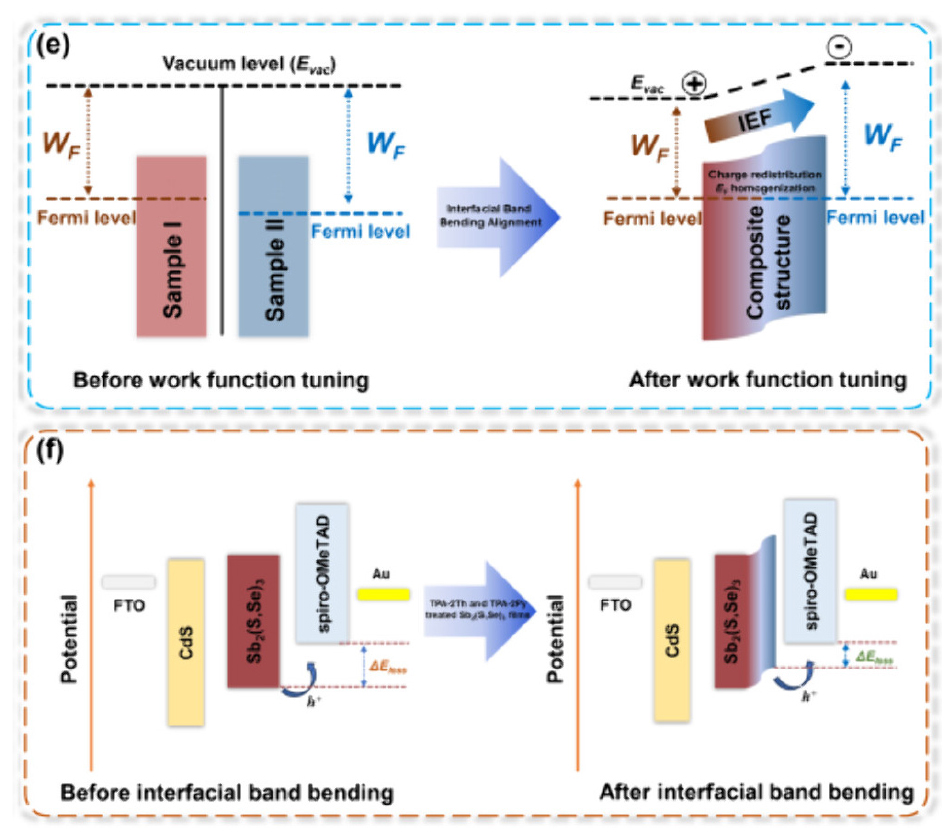
Fig. 1
Interfacial band bending mechanism in the Control and and TPA-2Th- and TPA-2Py-treated Sb2(S,Se)3 films23). Non-exclusive license granted by publisher
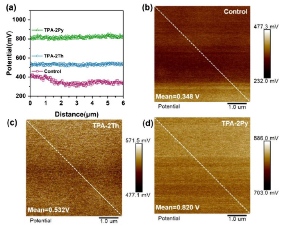
Fig. 2
KPFM images of Control and TPA-2Th- and TPA-2Py- treated Sb2(S,Se)3 films23). Non-exclusive license granted by publisher
4. Conclusions
Interface engineering remains central to unlocking the efficiency and stability potential of antimony chalcogenide (Sb2(S,Se)3/Sb3Se3) thin-film solar cells, where recombination at the heterojunction and especially the back contact can still limit open-circuit voltage and fill factor. Recent progress shows that both organic and inorganic hole-transport layers can provide favorable band alignment and defect passivation; for example, CuSCN and PbS colloidal quantum dot (CQD) HTLs, and transition-metal oxides such as V2O5 or NiOx, as well as all-inorganic MnS, have each been demonstrated to improve device performance and/or stability. Complementary back-contact and interfacial-layer strategies (e.g., interfacial modification, oxygen exposure, carbon electrodes, and flexible/back-interface trap engineering) further reduce contact barriers and mitigate deep-level defects. Combining scalable deposition with systematic energy-level control, interface passivation, and rigorous stability testing will be key for translating lab-scale advances into reliable devices.