

1. Introduction
2. Materials and Methods
2.1 Stacked Metallic precursor preparation
2.2 CZTSSe absorber preparation
2.3 Device fabrication process
2.4 Analysis of CZTSSe thin films and devices
3. Results and discussion
3.1 Compositional and morphological properties
3.2 Optical and electrical properties
4. Conclusions
Conflict of Interest
1. Introduction
The growing energy demands in forthcoming years to reach almost 30-40 terawatts are predicted by the year 20501,2). Therefore, finding sustainable energy sources that can overcome carbon emissions and fulfill energy demands is necessary. Solar energy can be a suitable renewable source of energy that can satisfy these demands. The CIGS and CdTe thin film solar cells (TFSCs) have already achieved device power conversion efficiency (PCE) of over 22% and are already commercialized3,4). However, the toxicity of Cadmium (Cd) and scarcity of Indium (In) and Gallium (Ga) elements encouraged the researcher to develop an earth-abundant element-based, low-cost, and nontoxic element-based alternative absorber layer5-7). Accordingly, the kesterite-based Cu2ZnSn(Sx,Se1-x) CZTSSe absorber layer exhibits earth-abundant elements, high absorption coefficient (105 cm-1), a tunable bandgap (Eg) ranges from 1.0 to 1.5 eV, and making them one of the suitable light absorber materials for TFSCs8,9).
Recently, CZTSSe-based TFSCs have achieved a record PCE of 13.8%10). However, the device performance of pure sulfide-based Cu2ZnSnS4 (CZTS) having record PCE = ~11.0%, pure selenide-based Cu2ZnSnSe4 (CZTSe) having record PCE = ~12.5%, and mixed chalcogenide (CZTSSe) is limited by the formation of defects, secondary phases, and associated charge carrier recombinations11,12). Most of the record efficiency devices exhibit non-stochiometric Cu-poor and Zn-rich conditions. At the same time various secondary phases, such as Cu2SnS/Se3 (CTS/Se), CuS/Se, ZnS/Se, and SnS/Se have also been observed in this Cu-poor and Zn-rich composition conditions11,13). They mainly originate from thermodynamically unstable single phases of CZTS and sulfur (S) rich conditions14,15). Although pure sulfide CZTS-based devices exhibit a wider Eg of 1.5 eV, they typically suffer a higher open-circuit voltage (Voc) loss8). On the other hand, pure selenide CZTSe-based device has a narrow Eg of 1.0 eV than the theoretically estimated maximum PCE of kesterite device (~32%), limiting their further development16). Lately, kesterite CZTSSe-based TFSCs have demonstrated their applicability in tandem configuration17,18). To employ kesterite absorbers in tandem solar cell device applications, it is essential to finely tune their Eg for efficient light absorption. Therefore, having a suitable Eg, optimum S/(S+Se) ratio, and fine Eg tuning strategies are needed for efficient light harvesting in PV devices.
In this work, the CZTSSe absorber layers were successfully deposited by the direct-current (DC) sputtering method, and a fine-tuning of the Eg was done by altering the S/(S+Se) ratio. Firstly, the composition and morphological properties of the CZTSSe absorber layer were evaluated, and later on, the influence of the S/(S+Se) ratio on optoelectronic properties was investigated by fabricating CZTSSe TFSCs with different S/(S+Se) ratio. The detailed investigation and obtained results are discussed below.
2. Materials and Methods
2.1 Stacked Metallic precursor preparation
The molybdenum (Mo) coated soda-lime glass (SLG) substrates of 2.5 × 2.5 cm2 were cleaned with an ultrasonication process sequentially with isopropyl alcohol (IPA) and deionized (DI) water for 15 min and dried under a nitrogen gun. Further, the cleaned Mo substrates were subjected to DC sputtering, and a precursor with stacking order of Cu/Sn/Zn/Mo was prepared. The sputtering power of 0.68 W/cm2 was used for all the targets while sputtering. Pure metallic targets with 99.999% purity purchased from (i-TASCO, USA) were used for all the processes.
2.2 CZTSSe absorber preparation
The prepared precursor layers were initially soft-annealed at 300℃ for 60 min in an Ar atmosphere within the tube furnace. Soft-annealed precursor thin films were annealed in a chalcogenide atmosphere with mixed S and Se powder (0.2 gm). The chamber was first evacuated to a base pressure of 1.0 × 10⁻⁵ Torr and then controlled up to 500 Torr using Ar gas before the annealing process. After that, the chamber was heated up to 520℃ with a ramping rate of 10℃/s, and the temperature was maintained for 8 min. The S/(S+Se) ratio of powder was changed from 0.02 to 0.08 to prepare the CZTSSe absorber thin films with different Eg. This 0.02 gm of S powder was mixed in 1.00 gm of Se chunks and grind well to make it homogeneous. Similarly, other powders were prepared by changing the S amount. It should be noted that all the samples were sulfo-selenized at the same conditions with the same amount of powder.
2.3 Device fabrication process
The CZTSSe devices were successfully fabricated by depositing the multi-layered structure of Al/AZO/i-ZnO/CdS/CZTSSe/Mo/SLG. The p-n junction was fabricated by depositing a ~60 nm thick CdS as a buffer layer using the chemical bath deposition (CBD) technique. The deposition was performed with a precursor of 1.5 mM CdSO4, 2.871 M ammonia, and 50 mM thiourea at 60℃ for 14 min and then rinsed in DI water. Further, the transparent conducting oxide (TCO) layers, i.e., i-ZnO and Al-doped ZnO-based (AZO), were deposited by radio-frequency (RF) sputtering technique at room temperature (RT) and 350℃ (real temperature 210-220℃), respectively. The thickness of i-ZnO and AZO were maintained at 30 and 550 nm, respectively. Finally, the Al top grid (1 µm) was deposited using the DC sputtering technique with the active area of the fabricated CZTSSe TFSCs to 0.30 cm2. Detailed thin film deposition and device fabrication processes can be found in our previous reports19,20).
2.4 Analysis of CZTSSe thin films and devices
The compositional ratio of the CZTSSe thin films was characterized by an X-ray fluorescence (XRF) spectroscopy (Axios Minerals PANalytical Netherlands). The surface morphology of the thin films was characterized using a field emission scanning electron microscope (FE-SEM, Model: JEOL JSM-6701F, Japan). The PCE for solar cell devices was characterized by a class AAA solar simulator (WXS-155S-L2) with the condition of AM 1.5G, 100 mW/cm2, and 25℃. The devices' external quantum efficiency (EQE) was measured using a QEX10 spectral response system (S-9230, SOMA Optics, Japan).
3. Results and discussion
3.1 Compositional and morphological properties
To determine the effect of the S/Se ratio on the composition ratio of the CZTSSe absorber layers XRF measurements were performed, and the corresponding results are shown in Fig. 1 (a)-(d). It shows that, with the change in the S/Se ratio during the sulfo-selenization process, the relative metal composition ratio Cu/(Zn+Sn) remained nearly stable ~0.65 - 0.66. At the same time, the Cu/Sn and Zn/Sn ratios increased initially with increasing the S/Se ratio from 0.02 to 0.06 and then decreased to a higher S/Se ratio of 0.08 (Fig. 1 (a)). The Zn/Sn ratio increased from 1.35 to 1.39 and then reduced to 1.36. Similarly, the Cu/Sn ratio increased from 1.40 to 1.44 and decreased slightly to 1.43 (Fig. 1 (b)). In the case of the chalcogenide to metal (S+Se/M) composition ratio, it nearly remained constant (Fig. 1 (c))14). The S/(S+Se) and Se/(S+Se) ratios also increased and decreased linearly with an increase in S and a decrease in Se content within the CZTSSe absorber layer, respectively (Fig. 1 (d))15). During the experiment, the metal (Cu-Zn-Sn) composition ratios for all the precursor layers were kept constant; thus, the change in the S/Se ratio was not significantly influenced. However, the possible formation of various secondary phases such as ZnS/Se, Cu2Sn(S/Se)3, and Cu(S/Se), potentially affected the Zn/Sn and Cu/Sn ratios11). The occurrence of these secondary phases is attributed to the thermodynamically unstable nature of CZTSe and CZTS absorbers due to their off-stoichiometry composition and a higher S/(S+Se) ratio21,22). Further, for the sulfo-selenization process, a fixed amount of S/Se mixture powder (0.2 gm) was used; hence the relative (S+Se)/M composition ratio for the CZTSSe absorber layer also remained constant. These measurements shows that can be seen that the overall composition ratios of the absorber layer do not get deflated by the change in the relative S/(S+Se) ratio23).
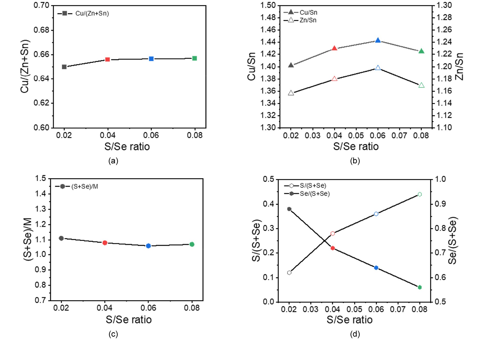
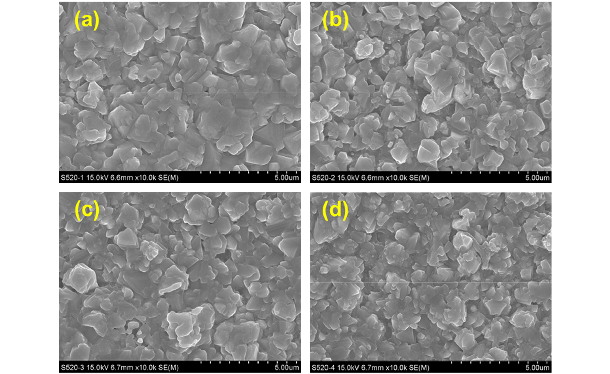
Fig. 2 (a)-(d) shows surface FE-SEM images of the CZTSSe thin films fabricated with different S/Se ratios. Surprisingly even though the metal composition of the precursor layers didn’t change after the sulfo-selenization process, the changes in the absorber morphology with the different S/Se ratios were observed. At a lower ratio of 0.02, the CZTSSe absorber shows much larger grains with compact morphology. While, at a higher S/Se ratio of 0.08, the density of smaller grains and voids increased. This poor morphology, associated with increased S/Se ratio, may be attributed to higher S content in CZTSSe thin films and a shorter sulfo-selenization time during the rapid thermal annealing (RTA) process15). These smaller grains increase defects and grain boundary density in the kesterite CZTSSe absorbers and can contribute to higher carrier recombination reducing device performance12,25,26).
3.2 Optical and electrical properties
To further evaluate the effect of the S/Se ratio on the performance of the CZTSSe devices, the device performance was measured under STC, and the corresponding data is shown in Fig. 3. As can be seen in the figure, the Voc and short circuit current density (Jsc) of the CZTSSe devices get linearly increased and decreased with increasing the S/Se ratio from 0.02 to 0.08, respectively. At the lower S/Se ratio of 0.02, the average Voc of the device remained up to 439 mV which increased further to 460 and 489 mV for 0.04 and 0.06 S/Se ratios, respectively (Fig. 3 (a)). When the ratio increased to 0.08, the Voc of the CZTSSe devices reached over 500 mV delivering an average Voc of 506 mV. It is known that the Voc is directly related to the Eg of absorber materials; therefore, increasing S content leads to an increase in Eg and an increase in Voc of the CZTSSe device14,27). On the other hand, the average Jsc of the devices decreased linearly from 34.3 to 29.04 mA/cm2 when the S/Se ratio increased from 0.02 to 0.06 (Fig. 3 (b)). The highest ratio of 0.08 marginally reduced up to 27.99 mA/cm2. The change in Eg values is the reason for the increase in Voc and decreases in Jsc values for different S/Se ratios27). The average fill factor (FF) of the CZTSSe devices initially reduced from 54% to 44%, whereas it increased marginally to 50% (Fig. 3 (c)). Following the same trend, the average PCE of CZTSSe devices also decreased from 8.17% to 6.26%, from 0.02 to 0.06, respectively, and increased slightly to 7.01% at a S/Se ratio of 0.08 (Fig. 3 (d)). The series resistance (Rs) in the device also increased nearly two times from 11.2 Ω to 22.05 Ω with an increase in the S/Se ratio, while it decreased slightly to 17.5 Ω at 0.08. The shunt resistance (Rsh) also increased and decreased with increasing ratio. The increased Rs can be observed due to the formation of resistive Mo(S,Se)2 layer, degradation of absorber quality and possible formation of shunt paths near junction reason. The exact reason for this abnormal behavior is not known, though some additional investigations are needed. There is a tradeoff between the Rs and Rsh in devices. This initial decrease in FF and PCE could be attributed to the poor p-n heterojunction quality of the CZTSSe devices. The changes in the Eg values also vary the conduction band offset (CBO) values, and the possible increase in the CBO could severely impact the FF and PCE of CZTSSe devices28,29). The sudden increased device performance after degradation of FF and PCE can also be explained by the relatively lower Rs and higher Rsh values at 0.08 ratio, thus marginally high PCE and FF was observed. In kesterites, Zn-rich and Cu-poor case, highly resistive Zn-related secondary phases (ZnS/Se) are commonly observed which possess a wide Eg, consequently, they lead to a degradation in the PCE of CZTSSe TFSCs22,24). The highest device PCE of 8.46% was achieved with a S/Se ratio of 0.02% with Voc, Jsc, and FF of 442 mV, 33.99 mA/cm2, and 56%, respectively. Where the highest Voc of 514 mV was achieved with the highest S/Se ratio of 0.08, the corresponding device exhibits the highest PCE of 7.85%.
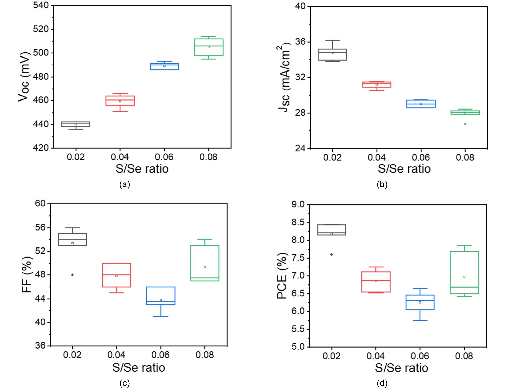
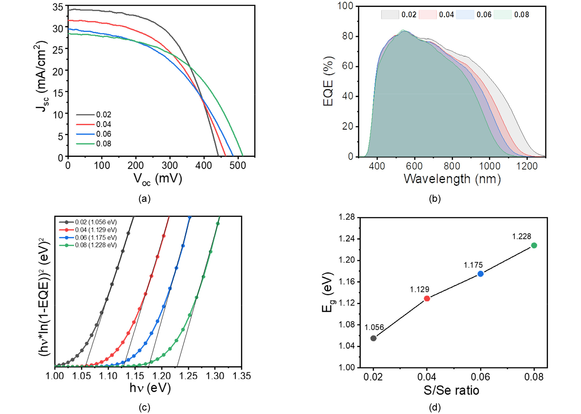
Fig. 4 (a) and Table 1 show the corresponding current-density-voltage (J-V) curves and device parameters. To validate the changes in Eg values with different S/Se ratios, the external quantum efficiency (EQE) for best-performing devices was measured. As shown in Fig. 4 (b), all the devices show strong absorption in the ultraviolet-visible (UV-Vis) region, ranging from 350 to 780 nm, decreasing further in the longer wavelength. All the samples exhibit a maximum EQE response greater than 80% without antireflection coating (ARC). With the increase in the S/Se ratio from 0.02 to 0.08, a significant shift in the absorption edge by approximately 200 nm in the longer region from ~1000 to 1190 nm was observed14). This blue shift corroborates well with the change in Eg values estimated by tracing the inflection point of the EQE spectrum at the absorption edge (Fig. 4 (c)). The Eg values increased linearly from 1.056 to 1.228 eV linearly with increasing S/Se ratio from 0.02 to 0.08, respectively (Fig. 4 (d)). It has been shown that, as the S content in the CZTSSe thin films increases, it shifts the valence band maximum position towards higher binding energy side resulting in widening of Eg.
Table 1.
Device parameters of the CZTSSe devices prepared with 0.02-0.08 S/Se ratio
In one study, Singh et al.23) fabricated the CZTSSe thin films and investigated how the small amount of S and Se can control the Eg. They observed that with the increase in selenization time, the Eg decreases from 1.35 to 1.10 eV, due to the replacement of S by Se, respectively. Similarly, Kim et al.14) studied the effect of S/(S+Se) ratios on Eg and their influence on the formation of secondary phases of the CZTSSe solar cells. They also observed formation (960 nm) of thick Mo(S,Se)2 resulted in decrease in the S/(S+Se) ratio that led to poor carrier collection at the back interface.
4. Conclusions
In the present work, we have successfully demonstrated that the Eg of the CZTSSe devices can be finely tuned by changing the S/(S+Se) ratio. It was found that the change in the S/Se ratio from 0.02 to 0.08 does not modify the overall Cu/(Zn+Sn) metal composition ratio. While, S/(S+Se) and Se/(S+Se) within the CZTSSe absorber layer get linearly increased and decreased, respectively. The morphological studies revealed, the density of smaller grains also increased, and overall absorber quality decreased at a higher S/(S+Se) ratio for CZTSSe absorbers. The optical and electronic properties estimated for corresponding devices showed that the Voc and Jsc of the CZTSSe device also increased and decreased linearly with increasing the S/(S+Se) ratio. Further Eg values estimated from EQE showed a linear increase from 1.056 eV to 1.228 eV. The device PCE also gets degraded with increase in S/(S+Se) ratio, thus fine tuning of composition with an increase in the Eg, suitable CdS buffer layer thickness, and optimization of CBO are needed. It can produce high quality CZTSSe device with an improved carrier separation process. This study will help Eg engineering the CZTSSe absorber, making it highly suitable for next-generation tandem solar cell applications.
