

1. Introduction
Polycrystalline Cu(In,Ga)Se2 (CIGSe) absorber is one of the most promising photovoltaic materials, as their cell efficiency has steadily increased up to 23.35% on glass1). However, its rigid soda-lime glass (SLG) substrate limits its use on curved building and automobile applications. Therefore, alternative substrates have been utilized for flexible CIGSe solar cells. Several groups have achieved high efficiencies of flexible CIGSe solar cells with 21.4%2) and 20.56%3) for polyimide (PI) and stainless steel (STS) substrates, respectively.
In order to enhance the device performance, high-quality of CIGSe films should be obtained, and detrimental defects also need to be sufficiently suppressed. In this regard, CIGSe films have been grown by a three-stage process while the Ga grading in CIGSe films is controlled in terms of bandgap engineering. Then, it provides an improved band alignment and reduced recombination at interfaces, thereby improving the collection of photo-generated minority carriers4,5). In addition, alkali doping for CIGSe films has been widely applied to suppress harmful defects. Specifically, post-deposition treatment (PDT) method was adopted by supplying various alkali compounds including Na, K, Rb, and Cs6,7). However, as mentioned, to realize flexible solar cells, CIGSe films should be grown on flexible PI and STS substrates which are different from conventional SLG substrates. As a result, the deposition conditions for high-quality CIGSe film growth should be investigated based on the substrate material properties such as thermal and mechanical properties.
In this work, flexible CIGSe solar cells were fabricated on an STS substrate since its substrate has no limitation in process temperature compared with PI. However, Fe, i.e., a constituent element is known as a killer ion to form deep defect levels in CIGSe bulk, so that suitable process temperature which does not accelerate Fe diffusion needs to be found while employing a diffusion barrier. Moreover, the STS surface roughness is relatively high. It means that CIGSe film quality can be dependent on the STS surface. To overcome such unfavorable growth conditions, the introduction of Ag in the CIGSe film was considered. In general, low-melting-point Ag reduces crystallization temperature and alloying a small amount of Ag induces a negligible change in band gap8,9). This leads to improved crystallization and surface morphology, resulting in better film quality of the CIGSe films10). Herein, the optimal Ag content to grow high-quality CIGSe films has been investigated. When it comes to control over defect passivation, alkali PDT is known as the most effective way to improve defect properties of CIGSe films. Thus, heavy alkali RbF PDT combined with NaF PDT was introduced immediately after CIGSe film growth.
Consequently, when the 6 nm Ag was included in the film, the grain size of CIGSe became larger. In addition, the optimized alkali PDT conditions resulted in an improvement in device efficiency. The best cell on the STS substrate yielded more than 16% efficiency, comparable to the cell on an SLG substrate. It suggests that the Ag alloying combined with alkali PDT is essential to make high-efficiency flexible CIGSe solar cells.
2. Experimental method
100 μm-thick stainless steel foil (430 series) was used as a substrate. On top of the STS, 200 nm-thick Cr layer served as a diffusion layer to minimize Fe diffusion from STS substrate during high-temperature process. Then, ~800 nm-thick Mo back contacts were deposited onto clean STS substrates using DC magnetron sputtering method. To find an optimal Ag content in CIGSe films, the Ag layer thickness was adjusted from 2 to 15 nm by using a thermal evaporator. Next, CIGSe absorbers were deposited on STS substrates using a three-stage co-evaporation process followed by NaF and RbF PDT. The thickness of CIGSe films is approximately 2.0 µm showing a nominal composition of [Cu]/([In]+[Ga]) ~ 0.9 and [Ga]/([In]+[Ga]) ~ 0.34. Details on CIGSe film growth is shown in Figure 1. 60 nm-thick CdS films were prepared by a chemical bath deposition (CBD) method. Then, 50 nm-thick i-ZnO and 150 nm-thick indium tin oxide (ITO) films were sequentially deposited by RF sputtering method. Finally, 1 μm-thick aluminum grids as a front electrode were deposited using thermal evaporation. The structure of a flexible CIGSe solar cell on the STS is schematically displayed in Figure 2.


To characterize the properties of CIGSe films, scanning electron microscopy (SEM) and energy-dispersive spectroscopy (EDS) measurements were carried out using S-4800 (HITACHI, Japan). Light current density-voltage (J-V) curves were measured under standard test conditions (AM 1.5G at 25°C) using McScience solar simulator. External quantum efficiency (EQE) spectra were measured by McScience K3100. The capacitance-voltage (C-V) profiles were recorded using an Agilent-4284 Precision LCR meter at 100 kHz in the dark condition.
3. Result and discussion
Figure 3 shows SEM images of the plain and cross-sectional views of CIGSe films grown on STS and SLG substrates. When a small amount of Ag was incorporated in the CIGSe film by preparing the Ag layer on top of Mo back contact, the grain sizes of CIGSe became bigger compared to CIGSe grains without Ag alloying. Especially, the Ag-alloyed grains extended throughout the film which is desirable in terms of charge carrier separation without recombination. According to literature, Ag alloying lowers a eutectic point to form CIGSe film, facilitating an improved intermixing of constituent elements, thereby increasing CIGSe grain sizes8,9).
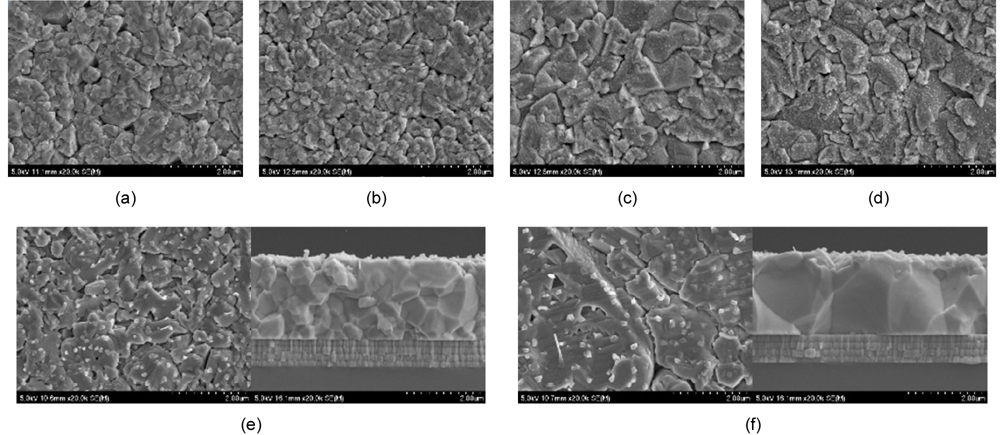
Fig. 3
Plain and cross-sectional SEM images of CIGSe films on STS and SLG substrates: (a) STS without Ag and alkali PDTs, (b) STS with the only Na PDT only without Ag doping, (c) STS with 6 nm Ag doping and Na PDT and (d) STS with 6 nm Ag doping and Na/Rb PDTs. As a purpose to probe effect of Ag alloying on the CIGS microstructure, (e) SLG with Na/Rb PDTs and (f) SLG with 6 nm Ag doping and Na/Rb PDTs.
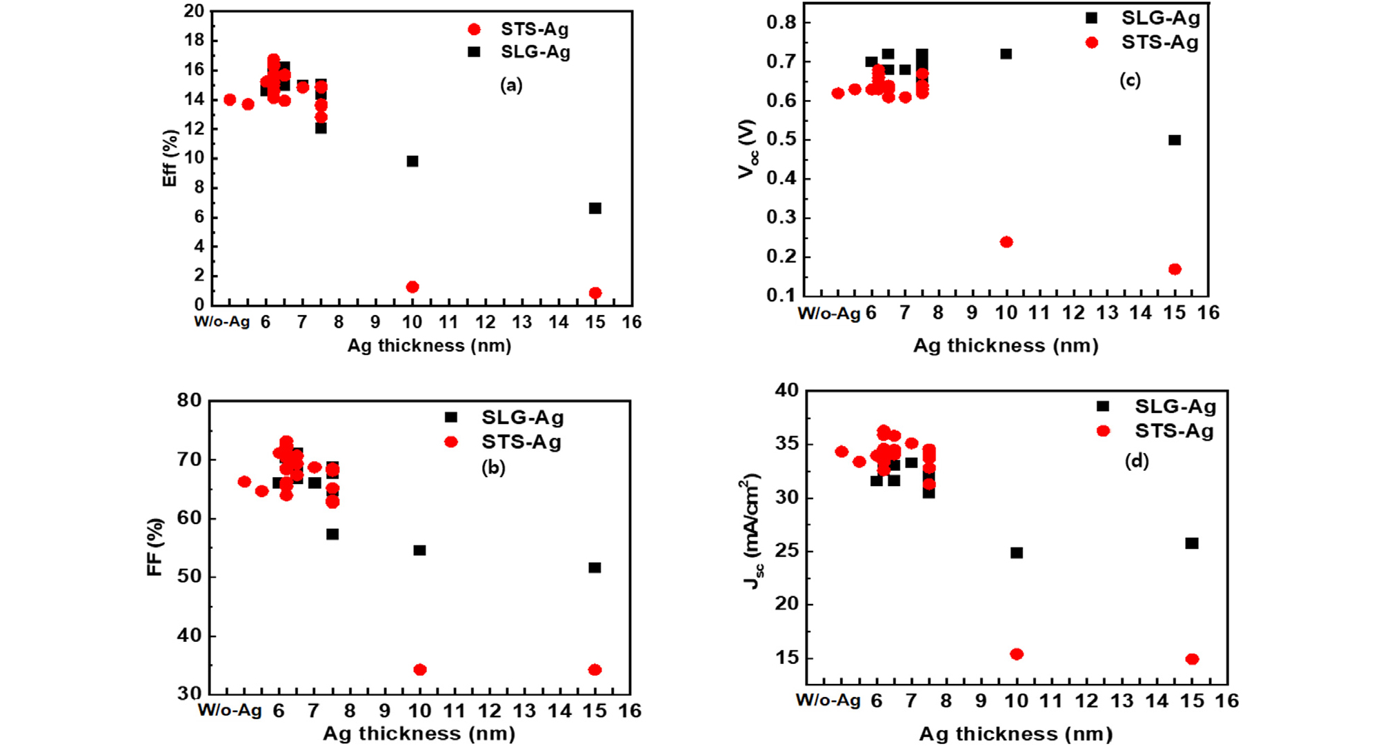
To find the optimal amount of Ag layer in the film, the thickness of Ag layer was adjusted from 2 to 15 nm as shown in Figure 4. The best efficiency of CIGSe cell was obtained from a 6 nm Ag layer. When the Ag amount was increased, the photovoltaic parameters were degraded. The open-circuit voltage and short-circuit current were seriously lowered, thereby decreasing the device performance. The decrease in PV parameters could be possibly caused by compositional non-uniformity on the CIGSe surface when Ag alloying content is increased in the CIGSe film. Some literature has already reported that segregation of secondary phases could result from uncontrolled Ag alloying, typically at the CIGSe surface11,12). Thus, the performance of solar cells might be adversely affected by the relatively high amount of Ag by secondary phases11,12). Despite such a small amount, it is essential to note that Ag plays a significant role in improving the microstructure of CIGSe films.
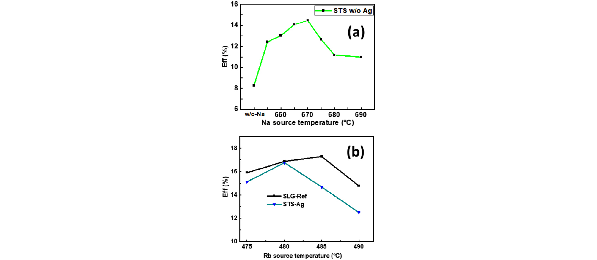
In addition to optimization of Ag inclusion, NaF and RbF PDT processes were optimized by adjusting the evaporation temperature of NaF and RbF sources. First of all, as shown in Figure 5, the NaF source temperature was changed from 660 to 690℃. As a result, the cell efficiencies were centered at 670℃ which is an optimal condition for NaF PDT. At the RbF source temperature of 480℃, the best efficiencies were shown up to more than 16%. Given this observed results, the process window of PDT process seems to be relatively narrow. Nevertheless, the optimized condition shows reproducible results.
As shown in Table 1, the photovoltaic parameters are summarized according to the optimization of Ag alloying and alkali PDT. Basically, the STS cell without the abovementioned processes yielded less than 10% with a low open circuit voltage (VOC) of 0.56 V. First, Na doping induced significant enhancement in the device efficiency from 8 to 14%. The improvement in VOC contributed to increased device efficiency. It indicates that only Na doping seems to suppress detrimental defects. When Ag was introduced, there was an additional increase in device efficiency. Finally, the best cell on STS with heavy alkali RbF PDT showed higher efficiency of 16.7%, which is about 0.6% lower compared to the efficiency of the reference cell on SLG, which is 17.29% efficiency.
Table 1.
Summary of photovoltaic parameters for flexible CIGSe solar cells depending on optimal Ag alloying and NaF/RbF PDT processes
Figure 6 shows C-V measurements plotted as 1/C2-V to determine the carrier concentration and built-in potential in the CIGSe solar cells for three devices, including STS-Na, STS-Na-Ag, and STS-Na-Ag-Rb. The net carrier concentrations for the devices determined at 0 V are 2.4 x10¹⁵, 2.6 x10¹⁵, and 3.6 x1015 cm-3 for STS-Na, STS-Na-Ag, and STS-Na-Ag-Rb CIGSe solar cells respectively. There is no significant change in carrier density for the three devices. However, the best cell with optimal Ag alloying combined with alkali PDT has gained improved built-in potential, as indicated for each device in Fig. 6. A higher built-in potential represents a stronger electric field and reduction in charge recombination at the depletion region, which is associated with increased VOC and resultant device efficiency.
Although we expect the built-in potential to be greater than the devices' open-circuit voltage, the extrapolated voltages are smaller than the open-circuit voltages of the STS-Na, STS-Na-Ag, and STS-Na-Ag-Rb devices shown in Table 1. This is because measurements of doping concentration and built-in potential in crystalline materials with a homojunction may be easily accomplished using capacitance-voltage (C-V) measurements. However, interpreting and extracting experimental data for thin film devices with multilayer interfaces and heterojunctions is challenging13). As a result, capacitance can be contributed by numerous layers and interfaces14,15). This may explain why Figure 6 exhibits a voltage axis intercept greater than 100 mV lower than the device's open-circuit voltage. However, having observed the trend in the built-in potential increase in Figure 6, the plot could indicate device quality improvements by combining Ag precursor and Alkali PDT doping. Moreover, The inverse square of the capacitance (1/C2) plot against the voltage for the RbF alkali-doped device intersects with the other graphs at reverse bias voltages. As can be observed from the plot, the graph begins to flatten at small reverse bias voltage, which indicates the decrease of the 1/C2 slope for the RbF doped device. Therefore, as the doping concentration is inversely related to the slope, the doping concentration will increase in the reverse bias. Thus, the alkali RbF doping seems to affect the doping concentration in this device.

4. Conclusions
In this work, Ag precursor layer thickness was tuned from 2 to 15 nm to fabricate high-efficiency flexible CIGSe solar cells grown on stainless steel (STS) foil. Furthermore, the addition of Na and Rb alkali elements was optimized by varying source temperatures to enhance the performance of CIGSe solar cells. As a result, an optimal 6 nm Ag precursor layer incorporated into CIGSe film improved the CIGSe grain size as well as the cross-sectional microstructure. The optimized alkali PDT conditions, along with the optimal Ag layer, induced improvement in device efficiency. The best cell on the STS substrate yielded more than 16%, which is higher than the cell on the SLG substrate. Interestingly, as we demonstrated by capacitance-voltage measurements, Ag alloying improved carrier collection, increasing built-in potential. Therefore, the combined optimization of Ag alloying and alkali PDT plays crucial role in the fabrication of high-efficiency CIGSe solar cells on flexible substrates.
