

Subscript
1. Introduction
2. Fabrication of TOPCon solar cells
3. Background of the Progress
4. TOPCon Solar Cell Structure
5. Process of TOPCon Solar Cell
5.1 Ultra-Thin Oxide Layer
5.2 Poly silicon Doped Film
5.3 TOPcon cell efficiency progress
5.4 Loss factor analysis
5.5 TCAD analysis of bifaciality and conversion efficiency with n-type TOPCon solar cell
5.6 Analysis of interfuse concentration
6. Conclusions
Subscript
PERC : Passivated Emitter and Rear Cell
IBC : Interdigitated back contact
TOPCon : Tunneling oxide passivated contact
LPCVD : Low pressure chemical vapor deposition
PECVD : Plasma enhanced chemical vapor deposition
APCVD : Atmospheric pressure chemical vapor deposition
1. Introduction
The efficiency of traditional manufacturing solar cells has improved by 0.5 to 0.6% per annum and is now over 22% with the passivated emitter rear cells (PERC) structure in last few years1-3). When the Si solar cell’s efficiency approaches 23%, most of the recombination loss is due to metal contact. Therefore, contact passivation has been an enthusiastic investigation matter of photovoltaics for several decays. Of the various resources and compositions studied, the TOPCon4) remains the industry’s greatest interest. In TOPCon design, the metal does not come into direct contact with the wafer. Alternatively, a thin tunneling oxide is applied, followed by a layer of highly doped with n or p poly silicon that contacts the metal at the ends. Behind the tunneling oxide does not affect the operation of the device, as the tunneling oxide blocks one type of carrier. Therefor, these structures are commonly referred to as the passivating contacts. SunPower Corporation was fabricating the Integrating Back Contact (IBC) cells in 20105), where the contact use the passivating contacts. TOPCon cell of Fraunhofer ISE with an efficiency of 25.8%6, 7), and POLO-IBC with an efficiency of 26.1%8) were reported, where a specific surface area was 4 cm2. Inspired by these excellent research advances, attempts to introduce passive contacts into industrial solar cell manufacturing are fascinating. However, there are some industry requirements to consider. Firstly, it should currently use a large silicon wafer of 156.75 × 156.75 mm2, 161.7 × 161.7 mm2 or more. Secondly, we need a high-yield poly silicon deposition system. However, there are about three different techniques considered for large scale manufacturing: low pressure chemical vapor deposition (LPCVD)9), plasma enhanced CVD (PECVD)10), inline atmospheric pressure CVD (APCVD)11), and sputtering12). As far as the it knows, testing of continuous production of these deposition systems for the photovoltaic industry is still in its infancy. The third significant demand is the metallization to thin polysilicon film. High temperature screen printing is the industrial form of procedure. The challenge is to secure the thin tunnel-oxide/poly-Si layer from the annihilation of the firing-through paste at the elevated temperature. Firing from paste removes the polysilicon thin layer and introduces Ag nanoparticles into crystalline silicon that further enhance the saturation current Jo of the passivating contact region13). The saturation current density of the metal contacts was investigated about 35 fA/cm2.14) Polysilicon films with a thickness of more than 150 nm can withstand firing from extreme heat, on the other hand these polysilicon layers have a greater coefficient of absorption15) and initiate losses in absorption. Consequently, the development of appropriate pastes from metal is currently a challenge for the photovoltaic manufacturing. Regardless of present confronts, by the interpretation of the LCOE (levelized cost of electricity), n-type TOPCon cells are favorable contestants for mainstream after PERC efficiency extend up to 23%16, 17). Current information introduces a recently produced TOPCon cell from Research and Development section with a highest efficiency of 24.58% and an open circuit voltage of 716.8 reported in journal of elsewhere, these elements are currently mass-produced by many companies18).
2. Fabrication of TOPCon solar cells
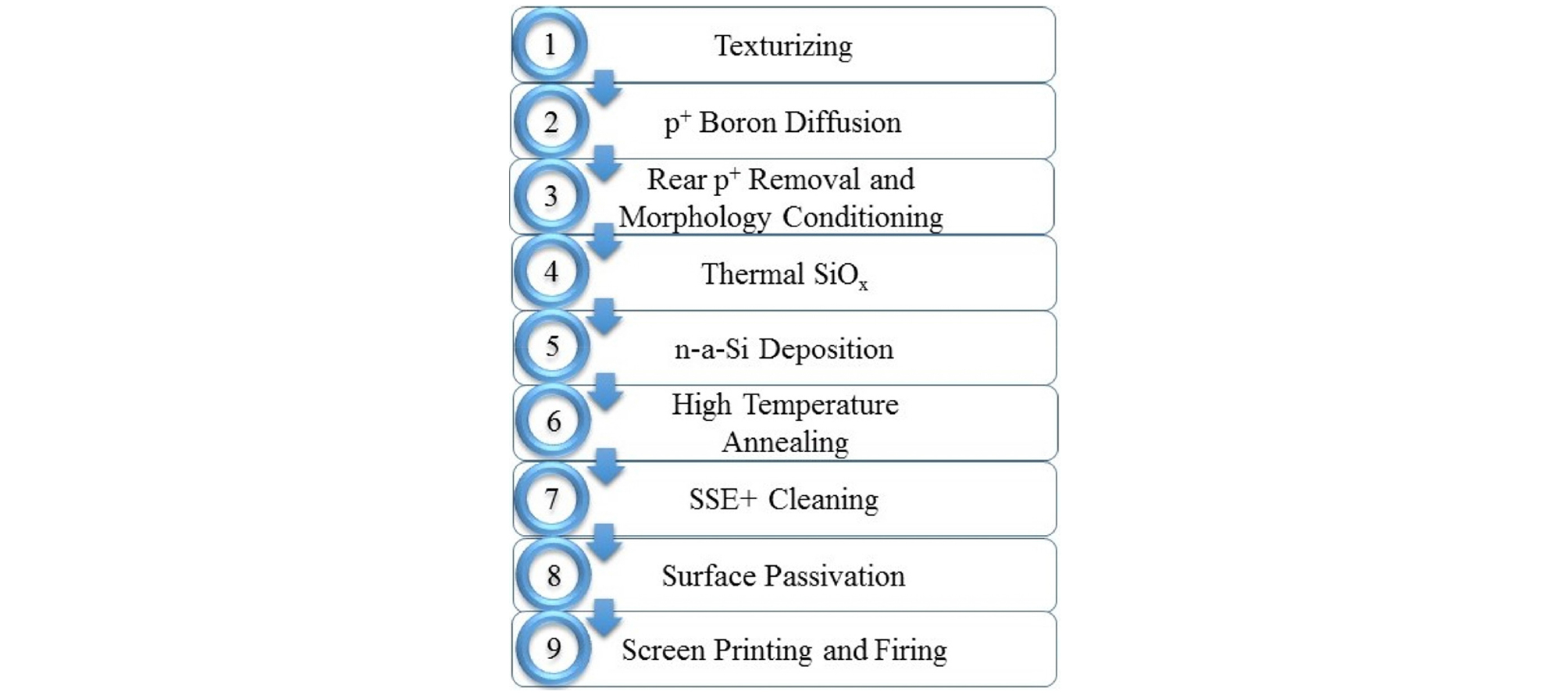
The construction assembly of the cell is demonstrated in Fig. 1. It constructs with boron emitter on front side and passivating connecting layer on back side, along with fingers on both sides pasted by screen-printed system to develop bi-facial solar cell. Low amounts of oxygen required for phosphorus doped wafers, with a resistivity level of around 0.5 Ωcm to 1 Ωcm. The sequence of cell construction is shown in Fig. 2. In a potassium hydroxide (KOH) solution the wafers are textured on both sides with irregular pyramids. After RCA cleaning, using a boron tribromide (BBr3) solution the boron emitter is created in a boron diffusion furnace. By a single side etching process using hydrofluoric acid and nitric acid (HF/HNO3) solution, the rear boron diffusion is removed. After cleaning with chemicals, a tunneling SiOx is thermally developed and a pure poly silicon layer (minimum partially poly-crystalline) is accumulated in a LPCVD system. The pure poly-silicon is doped in a phosphoryl chloride (POCl3) diffusion furnace consequently to transform into n+-poly-silicon. Additionally, etching process on single side is processed to eliminate the front side covered with poly silicon. The boron emitter is passivated with film of dielectric layer, subsequently additional RCA cleaning processed, that is correspondingly work as a coating of anti-reflection layer. The back side SiOx/n+-poly-silicon layer is covered with PECVD SiNx:H. For metallization, an “H-metal contact” design by screen printed on both sides with 9 bus-bars, afterwards a rapid firing procedure with a highest temperature of around 760°C17). The IV curve and other important parameters are deliberate with a suitable 1-sun (1000 W/m2) flasher instrument after construction of TOPCon solar cell.

3. Background of the Progress
The crystalline silicon solar cell has been thoroughly investigated for the previous some years. There is a high concentration of electrons in the location of the junction, thus the outcome is high loss of recombination of electrons in the solar cell, when the metal is in directly in-contact with the wafer of silicon. In the previous precedent, there were two approaches to reduce the carrier recombination of the metal precisely in contact with the silicon wafer: (1) by minimizing the interface capacity and by means of acquired smoothly doping; and (2) with employing a slight film of the passivated silicon level, to distinct the silicon wafer from the metal19-21).
The first point of the above approaches is a Passivated Emitter and Rear Cell (PERC), that is resulting from a traditional PN junction assembly, with native doping only in the emitter contact area. At present, its efficiency of current be able to attain highest as 22.8%22). The second point of the above process is Hetero-junction with Intrinsic Thin-layer (HIT) solar cell, explained by Panasonic company, these cells are presently described about 26.7% efficient22, 23).
The TOPCon solar cell can additionally appear as resulting from the conventional PN junction construction, related to the advantages of the two methods presented above. In previous decades, because of admirable passivation, the TOPCon solar cell has develop most of the investigation around the scientific community. Fraunhofer Institute of Germany projected the n-type solar cell by complete distinct charge carrier selective back contact is a dual-faced connection solar cell, with a highest efficiency record about 26.7%22, 23). The highest efficiency is because of the point in which the n-type silicon has a greater impurity accepted gain, and the faults in the surfaces are completely passivated. Most of the information have established that resistance of the substrate among 1 and 10 Ωcm utilized for the TOPCon solar cell that can attain more than 25% efficiency21). To enhance the solar cell efficiency and reserve a procedure that can endure to be augmented, the charge carrier selective contact is utilized in the projected TOPCon solar cell.
In comparison with the traditional silicon type solar cell, the TOPCon solar cell attains the subsequent purposes:24, 25)
1.The extreme fine layer of oxides satisfied the dangling bond that appear at the surface of the single crystal, therefore that enhance the efficiency of conversion.
2.Depending on the conductivity type of the substrate the extreme fine oxide layer allows to quick electron or hole transfer.
3.In consequence of the extreme potential in conductivity of the heavily doped poly silicon, the resistance of the junction can be decreased and the current output could be improved.
4. TOPCon Solar Cell Structure
Fig. 1 show a fundamental layout of the TOPCon solar cell, mostly produce with a PN junction on the substrate of an n-type material21, 26).
The cell is passivated by an Aluminums oxide (Al2O3) fine layer on the surface of the P-type material, and is contains of a very fine layer about 2 nm Silicon dioxide (SiO2) tunneling layer and a strongly doped poly silicon film on the surface of N-type material27). The major characteristics of the TOPCon solar cell is passivation on surface by the tunneling oxide film, and the selective contact to attain an incredibly minimal amount of recombination from intensely doping of poly silicon layer. To allow most of the carriers to tunnel, the tunneling SiO2 layer needs to be thin enough for transport, however at the same moment, its field effect can avoid the minority carriers from transmitting28). The characteristics of passivation of the intensely doped poly silicon layer is diverse by attuning the rate of hydrogen concentration by physical vapor deposition (PVD), for example atomic layer deposition (ALD) or sputtering, or chemical vapor deposition (CVD), such as plasma enhanced chemical vapor deposition (PECVD), or low pressure chemical vapor deposition (LPCVD). The intensively doped poly silicon layer reveals decent quality of passivation, because of the huge quantity of hydrogen atoms in the poly silicon layer29).
5. Process of TOPCon Solar Cell
5.1 Ultra-Thin Oxide Layer
Operative methods for developing extreme fine layers of oxide for the TOPCon solar cell is about 1.4 to 1.5 nm comprise: thermal oxidation, wet chemical dipping, and ultra violet ozone cleaning (UV/O3) processing. As well as, the simplest method to produce the fine layer of oxide is wet chemical dipping in the solution of acidic mixture at more than 90°C temperature. The process of thermal oxidation can be additionally separated into wet and dry oxidation from oxygen, as per the utilization of oxidizing environment. Pure and dry oxygen used for dry oxidation from oxygen as an oxidizing atmosphere, and to form the oxide film, at high temperatures oxygen reacts directly with hydrazine gas. The moist oxygen is an extreme clear vapor of pure water as an oxidizing atmosphere, and to form the oxide film from the molecules of water and oxide on the surface reaction. Generally, the rate of oxidation for dry oxygen oxidation is lower than that of moist oxygen24, 27).
5.2 Poly silicon Doped Film
The massive doping of poly silicon layer is created by 1) by utilizing LPCVD accumulating a silicon layer, reconciliation with additional ion doping, or 2) by employing PECVD precisely consigning a layer of silicon doping film.
5.3 TOPcon cell efficiency progress
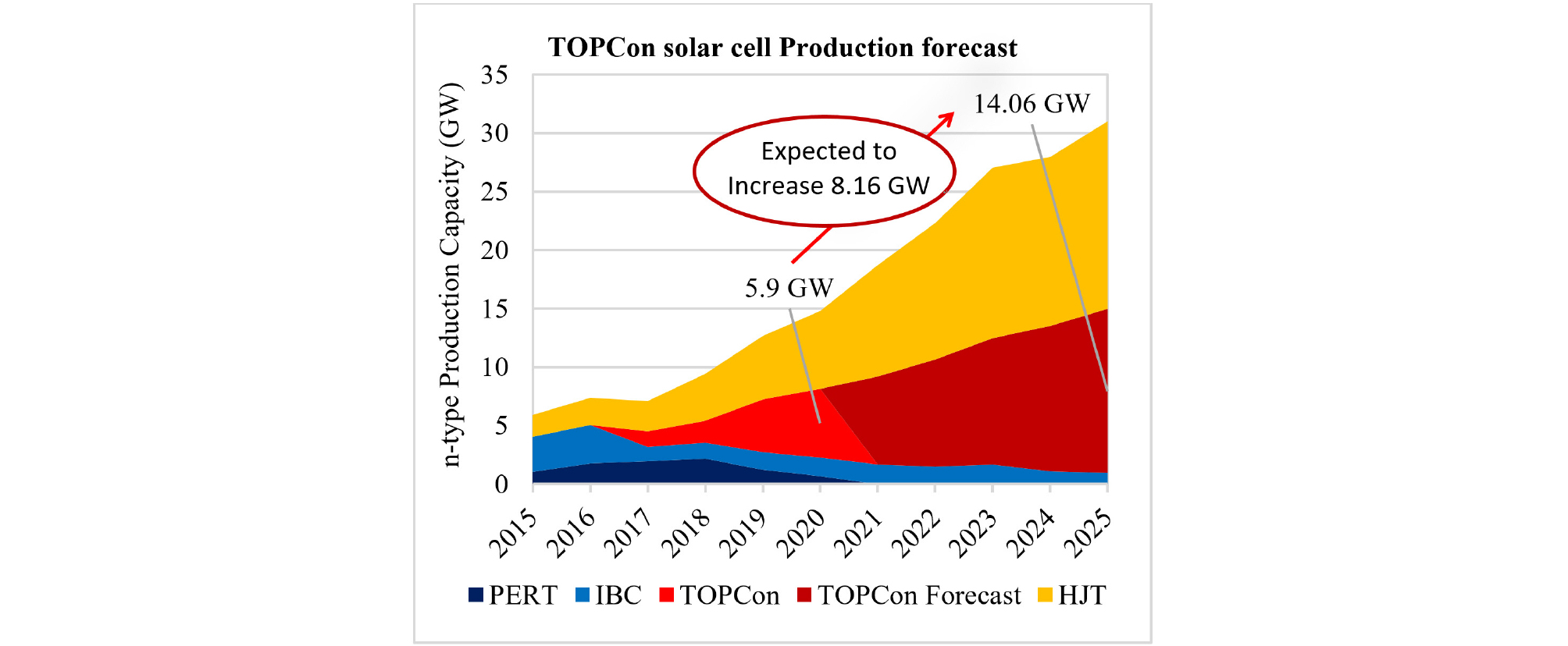
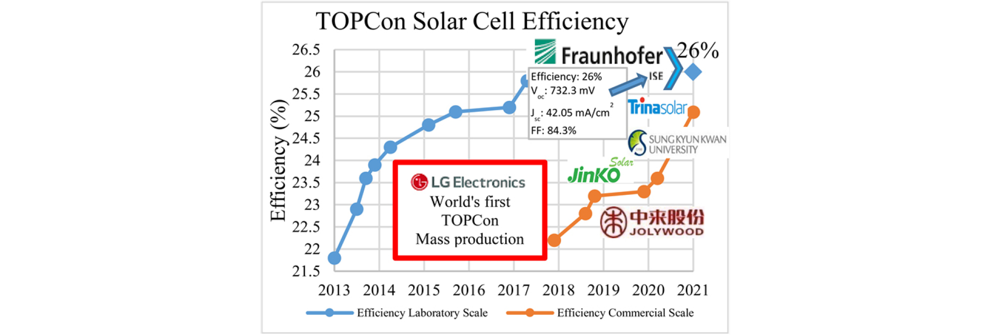
The TOPCon solar cell efficiency progress is explain in two categories one is the laboratory scale and other is commercial scale efficiency. The TOPCon solar cell efficiency was reported at laboratory scale on first and second quarter of 2013 about 21.8% and 22.9%, respectively, and in the third and fourth quarter of the same year the efficiency is improved and reported about 23.6% and 23.9%, respectively. In 2014 the efficiency of TOPCon solar cell was improved to 24.3%. In the last quarter of 2015, the efficiency was reported about 25.1%. In the laboratory scale the TOPCon solar cell got efficiency about 25.8% which is reported on 2017 by the Fraunhofer ISE as shown in Fig. 5. In the commercial scale the efficiency is reported in 2017 about 22.2% which was further improved to 23.2% on 2018. The scale of the efficiencies reach higher than before and got 23.3% on 2019 which if further enhanced on 2020 and stretched at 23.6% efficiency at the commercial scale. The conversion efficiency of N-type mono-crystalline based bifacial TOPCon solar cells had reached to 25.09%, which is the first crystalline silicon solar on a commercial size wafer exceeded the efficiency of 25% as shown in Fig. 3 and expected more than 28% after the year 2028. The efficiency is enhanced as the passivation technology improve and expected to increase the TOPCon solar cell production from 5.9 GW on 2020 to 14.06 GW on 2025 as described in the Fig. 4. The production capacity was expected to more than 8.16 GW30).

5.4 Loss factor analysis
The loss factors are classifying in 4 categories by bulk limit, optical, recombination and resistance loss. The bulk limit is recorded as 33% on which 5.35% loss due to bulk Jo at 10 fA/cm2 and efficiency reduce to 27.6% as shown in Fig. 6 (a & b) at point 1. The second factor is optical loss which is cause by the shading 0.65%, front reflection 0.38% and escape loss 0.02% that minimize the efficiency at 26.95%, 26.75% and 26.55% respectively which is shown in Fig. 6 (a & b) at point 2, 3 & 4. The third factor is the recombination loss that cause by the front passivation 0.37%, front contact 0.40% and rear passivation contact 0.11% that also lower the efficiency to 26.18%, 25.78% and 25.66% as described in Fig. 6 (a & b) at point 5, 6 and 7. The last loss factor is due to electrical resistance which is shunt resistance 0.10% and series resistance 0.46% that cause reduction in efficiency to 25.56% & 25.10% as revealed in the Fig. 6 (a & b) at points 8 & 9. The analysis of efficiency loss factor is described in Table 1 by the current density (mA/cm2), open circuit voltage Voc (v), fill factor FF (%), efficiency loss (%) and the final efficiency.
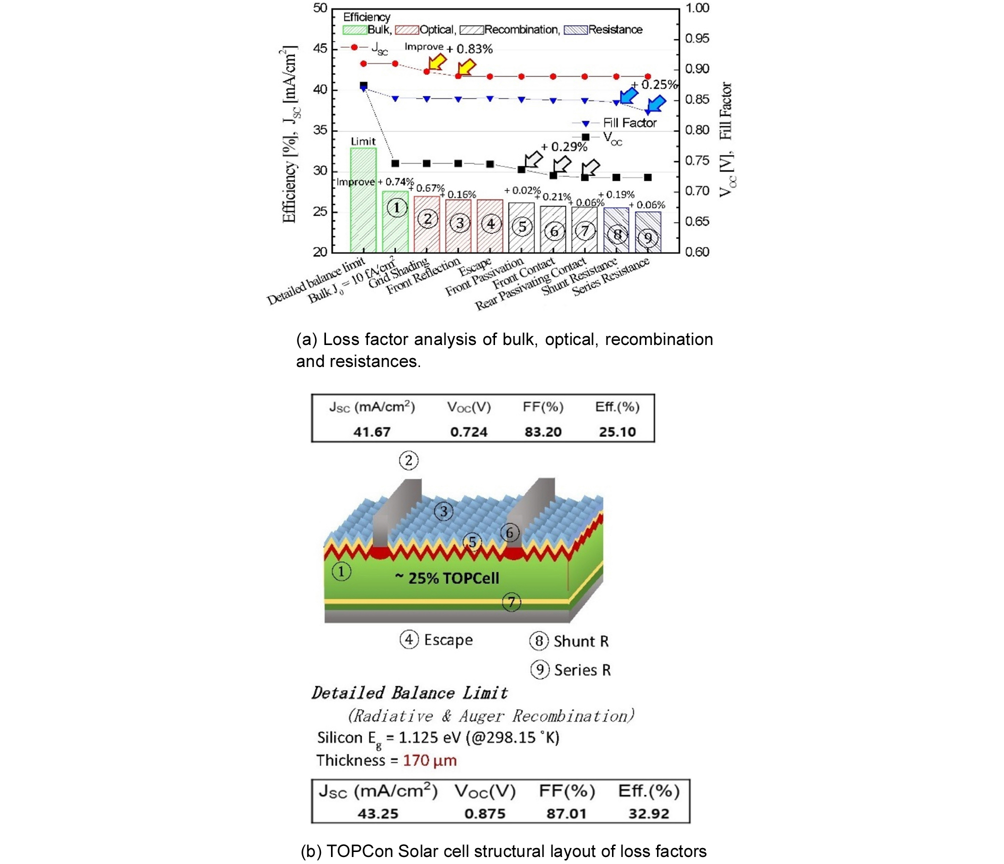
Table 1.
Analysis of efficiency loss by material
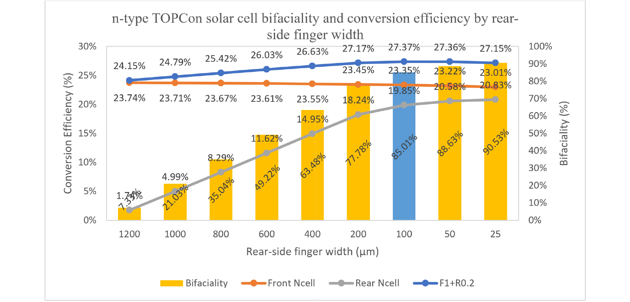
5.5 TCAD analysis of bifaciality and conversion efficiency with n-type TOPCon solar cell
The n-type TOPCon solar cell bifaciality and conversion efficiency is inspected by optimizing the finger width of rear-side contact. The TCAD analysis is conducted by changing the rear side finger width from 25 μm to 1200 μm and the efficiency on front & back side is observed and also bifaciality is calculated by dividing rear side efficiency to the front side efficiency. The efficiency is recorded at 25 μm rear finger width as 23.01% from front side and 20.83% from the rear side, the bifaciality at this width comes to be 90.53%. As the width of the rear side finger increase the efficiency of rear side of the cell drops significantly but the efficiency of front side of the cell increase slightly. The rear side finger width at 1200 μm, the efficiency of rear side of the cell drop up to 7.33% and the front side efficiency of the cell upsurge to 23.74% and the bifaciality is calculated as 1.74% due to low efficiency of rear side of the cell. As the rear side efficiency is dropped by increasing the rear side finger width and front side efficiency is increase when the rear side width is increase, so, we can identify the optimize value of the rear side finger width using F1+R0.2. Which means that sum up the 100% efficiency value from the front side and 20% efficiency value from the rear side efficiencies. The optimum value of the rear side finger width is 100 μm on which the rear side efficiency is 19.85% and front side efficiency is 23.35% and the optimum efficacy on both side is 27.37% get by F1+R0.2 as shown in the Fig. 733).
5.6 Analysis of interfuse concentration
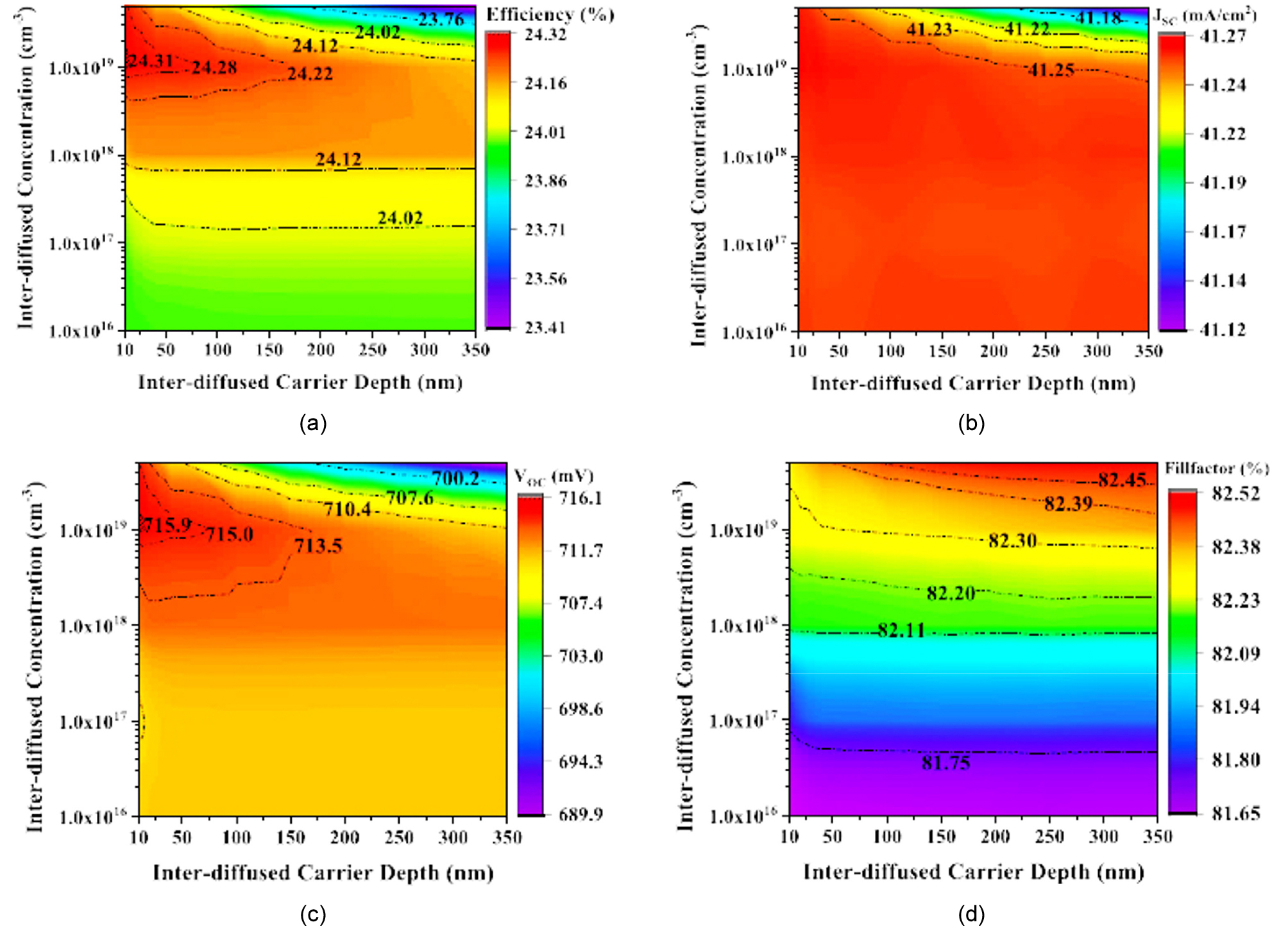
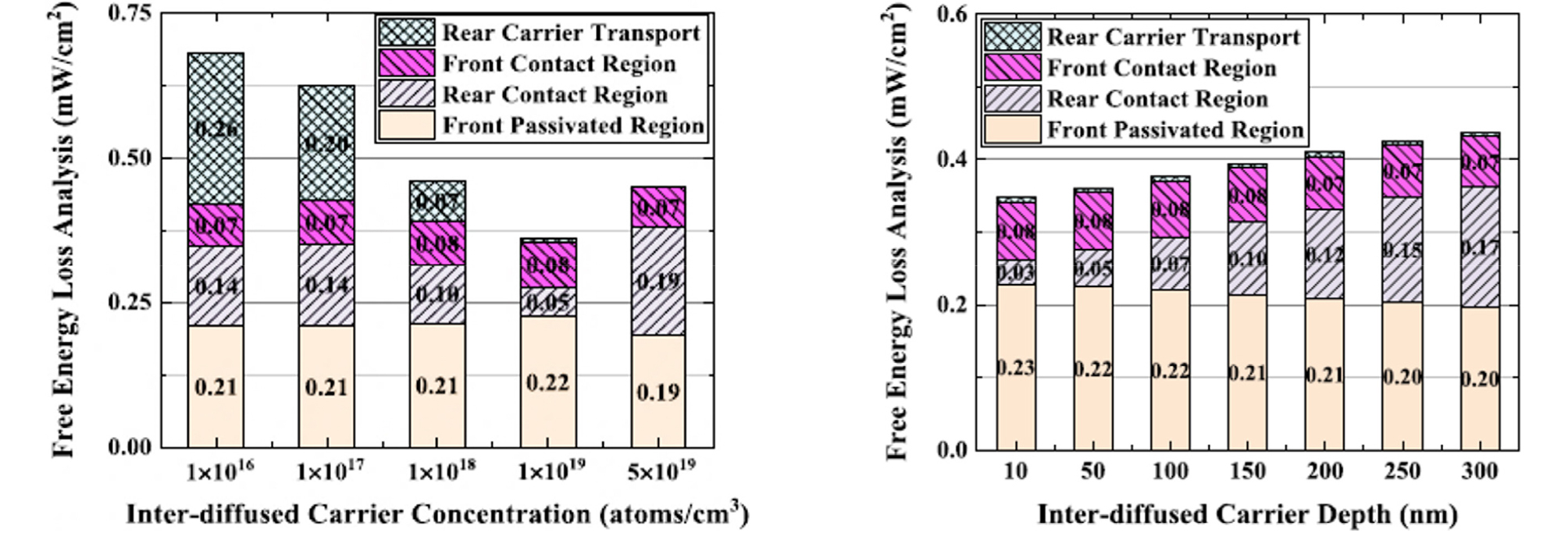
A contour graph is plotted between Inter-diffused carrier depth and inter-diffused concentration over various parameter like efficiency (%), current density (mA/cm3), open circuit voltage Voc (mV) and fill factor FF (%) as shown in Fig. 8. If the inter-diffused carrier depth is increased at same inter-diffused carrier concentration the efficiency will decreased. A high efficiency of 24.31% was obtained for the inter-diffused carrier concentration of 1×10¹⁹ atoms/cm3 at the depth of 10 nm as shown in Fig. 8(a). The current density decreases at the same inter-diffused carrier concentration when the inter-diffused carrier depth increased. So, at low depth high current density will be obtain at low concentration as shown in Fig. 8(b). A highest open circuit voltage Voc of 715.9 mV was obtained for the inter-diffused carrier concentration of 1×10¹⁹ atoms/cm3 at the depth of 10 nm as shown in Fig. 8(c). A fill factor FF (%) of 82.25% was obtained at highest efficiency for the inter-diffused carrier concentration of 1×10¹⁹ atoms/cm3 at the depth of 10 nm as shown in Fig. 8(d). The loss increases as the depth increases. The rear contact loss increases from 0.03 mW/cm2 to 0.17 mW/cm2 for an increase in inter-diffused depth from 10 nm to 350 nm. The impurity concentration was varied from 1×10¹⁶ atoms/cm3 to 5×10¹⁹ atoms/cm3, and the depth was changed from 10 nm to 350 nm in the TCAD tool as shown in Fig. 933).
6. Conclusions
In the advancement of TOPCon solar cells, it was contributory to utilize a sequence of trail tests and expounded investigation for attaining an autonomously inveterate successive efficiency of 24.58%. The stated efficiency is on larger wafer comprising bus bars and metal fingers, complete enlightenment, and fictitious with industrial manufacturing equipment. The review demonstrates that losses of recombination in the emitter, comprising its bulk, surface and metal contacts are restraining the implementation of the device, although the rear passivating contact has less Jo of not more than 7 fA/cm2, with the 94% non-metallized portion with Jo = 3.4 fA/cm2 in addition to 6% metallization section with Jo = 50.7 fA/cm2. It is accomplishing that enhancing the emitter and its metallization yet accepts a great ability for more improvements in efficiencies. This could be complete by advance progress of a traditional emitter construction and its metallization of paste, or by substituting it with a translucent passivating contact. In this review, abridging the performance of poly silicon passivating contacts, in addition to emerging a blatant passivating contact that is scientifically practicable, are currently highest imperative work in silicon photovoltaic investigation and progress. The solar industry is dominated by crystalline silicon solar cells. While interdigitated back-contact cell show the greatest efficiency, double-sided contacted cells are less complex and the recommended choice for industrial production. Avoiding the front side layer that providing lateral charge carrier transportation which is the key to the outstanding opto-electrical characteristics of the bi-directional cell. These consequences give a conversion efficiency of 26.0%. Unlike standard industrial cells which have a p-n junction at the front, the back of this cell has a p-n junction in the form of a full-surface passivation contact of polysilicon. Detailed analysis of power loss shows that these cells balances the electrons and hole transport losses, as well as typical transport losses and recombination losses. Systematic simulation studies have established some basic design rules for future silicon solar cells with efficiencies in excess of 26%, demonstrating the potential and superiority of these rear junction solar cells32).
