

Subscript
1. Introduction
2. Results and Discussion
2.1 Material systems and properties
2.2 Photovoltaics performance
2.3 Sub-module photovoltaics performance
3. Experimental Details
4. Conclusions
Subscript
PSCs : polymer solar cells
ETL : electron transport layer
ITO : indium tin oxide
NPs : nanoparticles
TAA-OH : nitrilotris(benzene-4,1-diyl)trimethanol
PCE : power conversion efficiency
RMS : root mean square
DIM : diiodomethane
DIW : deionized water
VOC : open-circuit voltage
FF : fill factor
o-XY : ortho-xylene
Ag : silver
MoO3 : molybdenum oxide
EQE : external quantum efficiency
μe : electron mobility
Jph : photo-current density
JSC : short-circuit current density
ZnO : zinc oxide
2-MTHF : 2-methyltetrahydrofuran
1. Introduction
Bulk-heterojunction (BHJ) polymer solar cells (PSCs) have gained considerable recognition due to low cost, lightweight nature, flexibility, and suitability for large-scale production. Significant progress has been made in the field of PSCs with power conversion efficiencies (PCEs) approaching 20%1–4). Meanwhile, PSCs with inverted structure have emerged as a compelling alternative to conventional architectures primarily due to their stable operational characteristics5, 6). In detail, the inverted configuration of PSCs positions the electron transport layer (ETL) beneath the photoactive layer. This design not only simplifies the fabrication process but also enhances device stability and compatibility with diverse electrode materials. Zinc oxide (ZnO), a widely studied ETL in this context, offers several benefits including high electron mobility, wide bandgap, and ease of processing7,8). However, despite these inherent advantages, the performance of ZnO-based PSCs is frequently compromised by some limitations related to interface quality, which demand further research to realize their full potential.
One significant issue with ZnO ETLs is the presence of various trap states within the material. These traps arise from intrinsic defects in the ZnO lattice, such as oxygen vacancies and zinc interstitials, and can impede charge transport by acting as recombination centers9). Additionally, hydrophilic nature of ZnO has poor compatibility with hydrophobic organic photoactive layers commonly used in PSCs. This mismatch in surface properties leads to suboptimal interface formation, inefficient charge extraction with increased recombination losses10, 11). The poor interfacial contact between ZnO and the organic photoactive layer not only affects charge transfer but also impacts the overall device efficiency. Therefore, enhancing the film interface quality to reduce shallow/deep trap states within the ZnO ETL is crucial for improving the performance of inverted PSCs. Several approaches have been investigated to address these challenges by modulating the surface properties of ZnO. One approach involves the incorporation of surface modifiers that can improve the compatibility between ZnO and the photoactive layer. Techniques such as employing self-assembled monolayers (SAMs)12, 13), ionic liquid molecules14, 15), alcohol/water-soluble conjugated polymers16), electron-rich polymers17), and polar organic solvents have been explored to modify the work function and surface energy of ZnO. SAMs, for instance, can form a monolayer on the ZnO surface that alters and improves the electronic properties at the interface with organic layers. Similarly, ionic liquids and polar solvents can interact with the ZnO surface to improve surface wettability and reduce energy barriers for charge transfer18). Despite the progress made with these surface modifiers, scalability and reproducibility remain significant challenges, often limiting their practical application in large-area device fabrication.
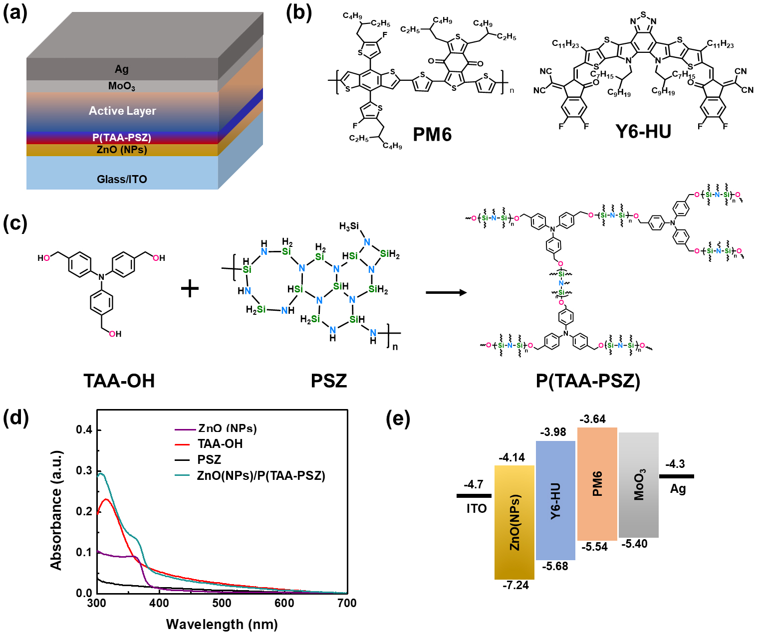
In this study, we propose an innovative solution to enhance the performance of ZnO ETLs by employing a cross-linked amine-based interlayer, poly(triarylamine-polysilazane) (P(TAA-PSZ)). This strategy is designed to address the aforementioned issues by creating a favorable interfacial contact that improves charge transport and reduces recombination losses. In detail, it lowers the surface energy of the ZnO ETL, improving adhesion between the hydrophobic active layer and the ZnO ETL. This modification effectively suppresses trap-assisted recombination and enhances charge transport and collection efficiency. The improved interface quality leads to a significant increase in the PCE of PSCs, from 14.26% to 16.31%. Additionally, the robust nature of the cross-linked P(TAA-PSZ) interlayer ensures its applicability in large-area sub-module fabrication, making it a promising candidate for scalable photovoltaic technologies. Overall, the results of this study emphasize the potential of P(TAA-PSZ) interlayer in advancing the field of polymer photovoltaics and contribute to the development of more efficient and stable solar energy harvesting technologies.
2. Results and Discussion
2.1 Material systems and properties
In this study, we fabricated PSCs with an inverted architecture as shown in Fig. 1(a). Glass/ITO was employed as the bottom transparent electrode and zinc oxide nanoparticles (ZnO NPs) was used as the electron transport layer (ETL). Above the ETL, P(TAA-PSZ) was coated as an interlayer to enhance charge extraction and improve interface stability. For the active layer, PM6 was used as the donor and Y6-HU was selected as the acceptor (Fig. 1(b)) due to their efficient charge generation/transport ability in ortho-xylene (o-XY) solution processing. Molybdenum trioxide (MoO3) was used as the hole transport layer, while silver (Ag) served as the top electrode. To prepare the P(TAA-PSZ) interlayer, nitrilotris(benzene-4,1-diyl)trimethanol (TAA-OH) was crosslinked with polysilazane (PSZ) under thermal treatment (110°C for 10 min in air). The ultraviolet-visible (UV-Vis) absorbance for ETL and crosslinking interlayers is shown in Fig. 1(d). The energy levels were measured by using cyclic voltammetry (CV) as shown in Fig. 1(c).
2.2 Photovoltaics performance
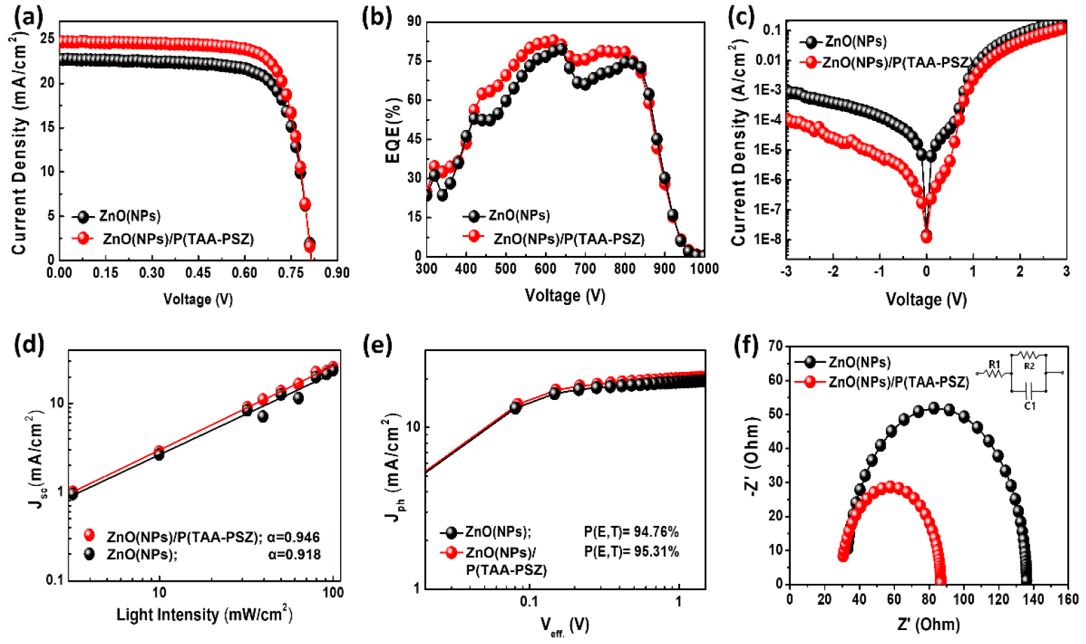
The fabricated devices demonstrated notable improvements in performance, with power conversion efficiencies (PCE) of 14.26% for the reference device and 16.31% for the device modified with P(TAA-PSZ), the device characterizations and photovoltaic performance are shown in Fig. 2(a)~(f) and Table 1.
Table 1.
Photovoltaic performances of the PM6:Y6-HU blend films via spin coating on small area
| Active Layer | ETL/Interlayer |
VOC (V) | JSC (JSC, calc)a (mA cm-2) |
FF (%) |
PCE (%) | Jd at −2 V (A cm-2) | α |
P (E,T) (%) |
|
PM6: Y6-HU | ZnO(NPs) | 0.80 | 22.68 (22.41) | 78.09 | 14.26 | 7.03×10⁻⁴ | 0.918 | 94.8 |
| ZnO(NPs)/P(TAA-PSZ) | 0.82 | 24.67 (24.17) | 79.96 | 16.31 | 2.54×10⁻⁵ | 0.946 | 95.3 |
The key photovoltaic performance parameters, particularly the open circuit voltage (VOC), short-circuit current density (JSC), and fill factor (FF), showed significant enhancement upon the inclusion of the interlayer. This improvement can be attributed to better charge extraction and reduced trap-assisted recombination18). The J–V characteristics are presented in Fig. 2(a), while the EQE spectra are shown in Fig. 2(b), demonstrating good spectral response across the visible range. The dark J–V curves in Fig. 2(c) indicates reduced leakage currents, confirming improved diode quality with the surface modifier. Moreover, the plot of Jsc versus light intensity were analyzed to assess bimolecular recombinations (Fig. 2(d))21), yielding slopes of 0.918 and 0.946 for ZnO and ZnO/P(TAA-PSZ)-based devices, respectively. These values demonstrate reduced bimolecular recombinations occur in the ZnO/interlayer devices due to improved contact between ZnO and active layer. To further investigate the impact of the ZnO and ZnO/interlayer on charge carrier dynamics, Jph–Veff. curves were obtained (Fig. 2(e))19). The charge collection probabilities, P(E,T), for the devices utilizing ZnO and ZnO/P(TAA-PSZ) were found to be 94.8% and 95.3%, respectively, indicating more efficient charge collection in the ZnO/P(TAA-PSZ) devices20). Lastly, electrochemical impedance spectroscopy (EIS) was performed in the dark to analyze the charge recombination properties (Fig. 2(f))23). The R1 and R2 values were determined from the EIS spectra, where R1 represents the ITO sheet resistance and R2 corresponds to charge-transfer resistance; thus, R2 can be associated with the interfacial resistance between the ETL and the active layer. First, the R1 values were found to be similar (i.e., 25.45 Ω for the ZnO-based devices and 24.94 Ω for the ZnO/P(TAA-PSZ)-based devices). However, the R2 value was found to be lower when the P(TAA-PSZ) interlayer was employed (i.e., 178.54 Ω for the ZnO-based devices and 155.74 Ω for the ZnO/P(TAA-PSZ)-based devices). As a larger semicircle indicates a higher R2 and more significant charge recombination at the ETL/active layer interface, it can be concluded that the P(TAA-PSZ)-based devices showed suppressed charge recombination compared to the reference devices without P(TAA-PSZ). These findings highlight the critical role of P(TAA-PSZ) interlayer in reducing recombination losses and improving the photovoltaic properties of the devices.
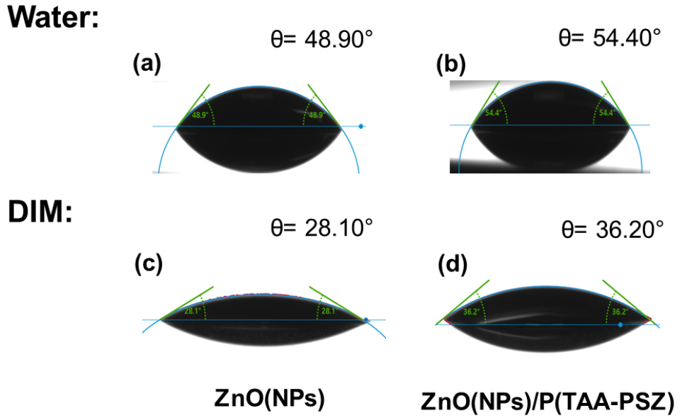
In addition to recombination studies, contact angle analysis was conducted to further understand the wetting behaviour of the ZnO and ZnO/P(TAA-PSZ) surfaces (Fig. 3). The contact angles were measured using water and diiodomethane (DIM), showing a slight increase for the ZnO/P(TAA-PSZ) indicating enhanced surface hydrophobicity. This shift in contact angle also corresponds to a decreased in surface energy from 57.5 mN m-1 for ZnO to 47.6 mN m-1 for ZnO/P(TAA-PSZ). The decrease in surface energy suggests improved adhesion between the organic active layer and the ZnO ETL, promoting more uniform coating24, 25). Moreover, these findings confirm that the crosslinking interlayer was successfully coated onto the ZnO layer, without interfering with the subsequent active layer deposition. This combination of decreased surface energy and increased hydrophobicity, along with suppressed recombinations and enhances interfacial contact, which is crucial for efficient charge transport and overall device performance.
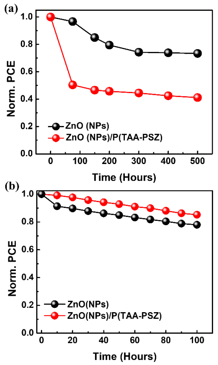
Additionally, in order to check the long-term thermal stability of the PSCs, we stored the devices in the dark at 80°C and monitored their PCEs for 500 h (Fig. 4(a)). The ZnO/P(TAA-PSZ)-based devices maintained ~72.97% of their initial PCEs after 500 h, while the ZnO-based reference devices retained only ~41.09% of their initial PCEs, mainly due to the JSC and FF degradation. The relatively hydrophilic ZnO-based reference devices suffer from poor interfacial contact with the hydrophobic active layer. This incompatibility may have promoted trap formation, interfacial recombination, and inefficient charge transport over time, especially under thermal stress. Therefore, this result highlights the effectiveness of the crosslinked P(TAA-PSZ) interlayer in enhancing device stability, which can be attributed to the optimized ZnO–active layer interface. In addition, we conducted a light-soaking stability test under continuous AM 1.5G illumination (100 mW cm-2) in an inert atmosphere for 100 h (Fig. 4(b)). As a result, the P(TAA-PSZ)-based devices retained ~85% of their initial PCE after 100 h, whereas the ZnO-based reference devices retained only ~78% of their initial performance, mainly due to the JSC degradation. These results confirm that the P(TAA-PSZ) interlayer also significantly improves the operational stability under light illumination, which is likely due to suppressed photo-induced trap formation at the interface.
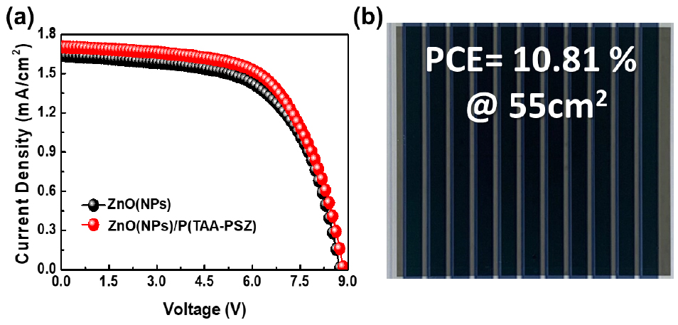
2.3 Sub-module photovoltaics performance
In addition to small-area devices, we have successfully fabricated a large-area sub-module with an active area of 55 cm2 on a 12×12 cm2 substrate. The fabrication conditions for the sub-modules were kept consistent with those used for small-area devices, ensuring a reliable comparison between them. The optimized large-area sub-modules exhibited PCEs of 8.69% for the ZnO-based ETL and 10.81% for the ZnO/P(TAA-PSZ) ETL, as shown in Fig. 5 and Table 2. This demonstrates a significant improvement in performance with the inclusion of the interlayer for large-area sub-module. Despite the up-scaling of the device area, the performance remains competitive, underscoring the robustness and scalability of the fabrication process. The enhancement in efficiency observed for the ZnO/P(TAA-PSZ) can be attributed to better charge extraction and reduced recombination losses, similar to the trends seen in small-area devices26–28). These results highlight the potential of the optimized ZnO/P(TAA-PSZ) ETLs for large-area organic photovoltaic applications.
3. Experimental Details
All reagents and solvent were purchased and used without any further purification, unless mentioned. Nitrilotris(benzene-4,1-diyl))trimethanol was synthesized by the procedure in literature29). The details regarding the fabrication of small and large-area PSCs and modules are as follows: the device structure consists of ITO/ZnO (NPs)/P(TAA-PSZ)/active Layer/MoO3/Ag. For the interlayer, TAA-OH was dissolved in 2-MTHF, while polysilazane was dissolved in dibutyl ether. Then, TAA-OH and polysilazane were mixed at room temperature, and subsequently coated on top of the ZnO layer and crosslinked through annealing at 110°C for 10 minutes in air (we note that the optimal device performance was observed with a 16 nm-thick P(TAA-PSZ) interlayer and a thermal annealing temperature of 110°C). The active layer solution was prepared by dissolving the PM6 donor and Y6-HU acceptor in o-XY with 1.0:1.2 w/w. After coating the active layer, thermal annealing was conducted at 110°C for 10 minutes inside a glove box. The thickness of active layer was ca. 130 nm. Spin-coating was employed for fabricating small-area solar cells, while bar-coating technique was used for large-area modules. For small-area devices, the active area was 0.12 cm2, while for large area sub-modules, the active area was 55 cm2. These complementary approaches enabled us to investigate performance across different device scales, providing insight into scalability and consistency of the fabrication process.
4. Conclusions
In this study, we have demonstrated a significant enhancement in the performance of inverted PSCs by addressing critical limitations associated with ZnO ETL. Our approach, involving cross-linking of an amine-based interlayer, has shown effectiveness in improving interface between ZnO and organic photoactive layer. This modification mitigates charge recombination and decreases surface energy of ZnO, resulting in better charge dynamics. As a result, the PCE increased from 14.26% to 16.31%, highlighting the substantial impact of this strategy on device performance. Furthermore, the robustness of the cross-linked amine-based interlayer demonstrates its practical applicability for large-area sub-module fabrication, addressing the scalability concerns often associated with surface modification techniques. Overall, our findings underscore the potential of using P(TAA-PSZ) to overcome the limitations of traditional ZnO ETL. This strategy offers a promising pathway for advancing PSC technology and could pave the way for more efficient and scalable solar energy harvesting solutions.
