

1. Introduction
2. Experimental
3. Results and Discussion
3.1 Optical characterization of In2Se3 thin film
3.2 Growth of In2Se3 on CIGS film
3.3 Zinc suppression in CIGS interface with an In2Se3 layer
3.4 Band structure of In2Se3/CIGS film
4. Conclusions
1. Introduction
Recently, an efficiency of 23.35% was reported in CIGS solar cells by employing Zn(O,S,OH)/ZnMgO double-layer buffer1), and 22% efficiency was reported by employing Zn0.8Mg0.2O buffer and Zn0.9Mg0.1O:B transparent conductive oxide layers2, 3). However, such results are still lower than the record efficiencies in Si and GaAs solar cells. The main cause of lower efficiency in CIGS solar cells is a low voltage gain ratio (~0.65) compared to those of Si and GaAs solar cells (~0.8), where the voltage gain ration is defined as qVoc/Eg, where q, Voc, and Eg are proton charge, open-circuit voltage, and band gap, respectively. In this respect, reducing the surface recombination rate in CIGS solar cells is one of the key factors to increase the voltage gain ratio.
In the CIGS solar cell, buffer layers including CdS, Zn(S,O,OH), ZnMgO, and ZnSnO have been introduced to increase the cell performance, especially, Voc. The CdS and Zn(S,O,OH) buffers were deposited by the chemical bath deposition (CBD) method. However, the CBD method is inappropriate for mass production due to uniformity issues, chemical waste treatment issues, and reproducibility problems. In this regard, the atomic layer deposition (ALD) process of buffers including ZnSO, ZnMgO, and ZnSnO is favorable because the ALD process could provide better uniformity in larger areas, better control of thickness, and less chemical waste. Somehow, most Cd-free buffers prepared by the ALD process have consisted of a Zn component in buffers. More details on Cd-free buffers and ALD process can be seen in a recent review paper4).
In general, compared to CIGS solar cells with CBD CdS buffer, CIGS solar cells with Zn-containing ALD buffers including ZnSO, ZnMgO, and ZnSnO buffers had lower open circuit voltage (Voc)4-6). During the ALD process, the CIGS substrate was heated for the ALD process to around 120°C, where Zn atoms diffuse into CIGS film through the copper vacancy sites7-9).
Fig. 1 shows the Zn depth profile in CIGS film after ALD ZnMgO growth at 120°C, which caused the Voc and FF of the CIGS solar cells to degrade in our previous report10). For this reason, the Zn diffusion into CIGS film should be prevented by introducing a diffusion barrier material in which Zn component is not included.
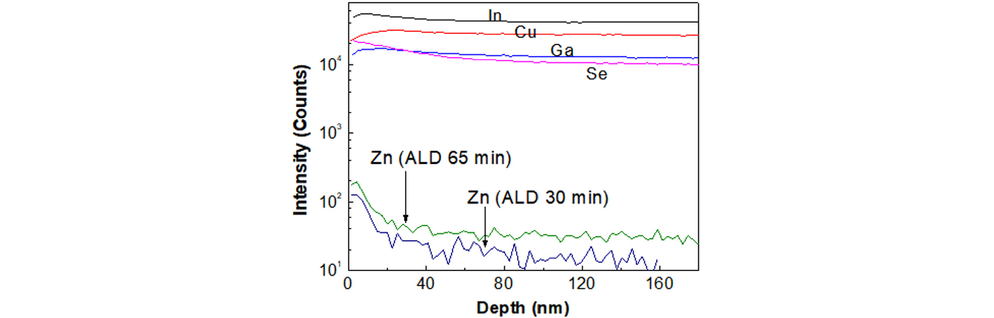
Fig. 1
Zn diffusion into CIGS film during ALD ZnSnO buffer growth at 120°C for two-different growing times10)
In the present paper, to prevent the Zn diffusion from ALD Zn-containing buffer to CIGS, we introduce an In2Se3 layer as a diffusion barrier on the CIGS surface. The main purpose was to prevent Zn diffusion from the Zn-containing ALD buffer during the ALD process because In2Se3 does not contain Zn atoms and can absorb Zn from Zn-containing buffers.
The second purpose was to reduce the interface recombination rate at the CIGS surface. The In2Se3 layer with a wide band gap can serve as a hole-blocking layer, like the commonly-used buffer layers in most CIGS solar cells. Commonly-used buffers employed in CIGS solar cells are either sulfides or oxides or oxygen-containing sulfides. The ionic radii of oxygen (0.132 nm) and sulfide (0.174 nm) are smaller than that of selenium (0.191 nm) so that interface between the commonly-used buffer and CIGS absorber can have many defects due to lattice mismatch, causing a high surface recombination rate. The examples of good lattices at the CIGS surface include a K(In,Ga)Se2 layer by NaF+KF PDT11, 12) and a Cu(In,Ga)3Se5 layer by Se PDT13). These layers, consisting of Se as the main matrix component, are a hole-blocking layer and epitaxy layer on CIGS film. However, a sturdier hole-blocking layer than those K(In,Ga)Se2 or Cu(In,Ga)Se2 layers is needed to achieve a higher voltage gain in CIGS solar cells. The band gap of In2Se3 is above 2 eV14, 15) and can have a hole-blocking barrier in contact with CIGS. Both In2Se3 and CIGS could have less interface defects because the matrix ions of both phases are Se ions, resulting in better lattice match than oxide- and sulfide-containing buffers. For example, CuIn3Se5 and CuInSe2 have the Se-based crystal matrix Therefore, CuIn3Se5 phase on CuInSe2 phase can have a partial epitaxial interface16). It was found that a better epitaxial interface was grown from the evaporation of molecular sources such as In2Se3 and Cu2Se16).
In adapting In2Se3 as a Zn diffusion barrier, one more restriction should be considered. Out-diffusion of copper from CIGS absorber to In2Se3 thin layer should be blocked to avoid forming CuInSe2 phase. The Cu concentration at the CIGS surface is high in the as-deposited CIGS film and low in the CIGS surface by Se PDT or NaF PDT13, 17, 18). Pure In2Se3 was successful grown at 300°C, and Zn diffusion into CIGS film was prevented by a 20-nm-thick In2Se3 layer. The details of In2Se3 growth on CIGS film, barrier characteristics on Zn diffusion, and a potential hole-blocking barrier are described in the Results and Discussion section.
2. Experimental
First, In2Se3 film was deposited by co-evaporation of In and Se elements on a glass or Mo substrate at 300°C to characterize the optical properties of In2Se3 film. The fluxes of indium and selenium were 0.8 and 1.5 nm/s, respectively. The deposition rate of In2Se3 thin layer was about 0.6 nm/s. For passivation purposes, In2Se3 thin layers with various thicknesses were deposited on the CIGS film by the same co-evaporation process on 1.8-μm-thick CIGS film that was also deposited by a three-stage co-evaporation process at 550°C13, 17). Then, 40-nm-thick Zn0.8Sn0.1O was deposited by ALD process at 120°C for 30 min, at which Zn could diffuse into CIGS through the In2Se3 passivation film19). The Zn0.8Sn0.2O composition was prepared by a 4:1 cycle ratio of ZnO ALD process (DEZ 0.1 s, purge 2 s, H2O 0.1 s, purge 3 s) and SnO2 ALD process (TDMA-Sn 0.1 s, purge 2 s, H2O 0.1 s, purge 3 s). With this experiment, we reported a 17.22% cell efficiency in the ZnSnO/CIGS structure without alkali post deposition treatment and AR coating19).
The microscopic image and composition of the films were examined by field-emission scanning electron microscope (SEM), transmission electron microscope (TEM), and electron dispersive spectroscopy (EDS) using FEI Nova23 with resolutions of 1.0 and 1.6 nm at 15 kV and 1 kV, respectively. The transmittance spectrum and reflectance spectrum were measured using a JASCO V-650 spectrophotometer at wavelengths ranging from 190 to 900 nm with an accuracy of 0.2 nm. The low-temperature photoluminescence (LTPL) spectra were measured at 10 K using LabRAM HR UV/Vis/NIR PL made by Horiba Jobin Yvon with a 514-nm laser. The wavelength of the laser source was 514 nm, and the power of the laser was controlled by filters. The x-ray photoelectron spectroscopy (XPS) of the Cu 2p3/2 spectra and valance band were measured using K-alpha made by Thermo VG Scientific. The Raman spectra of the films were measured using LabRAM HR Evolution Visible-NIR made by HORIBA. The depth profiles of elements in the films were measured by secondary ion microscopy (SIMS) with TOF-SIMS5 made by ION-TOF GmbH. Before depth profiling, the 40-nm-thick ZnSnO buffer on the films was etched by hydrochloric acid solution for about ten seconds to avoid a knock-on effect in CIGS film. With the chemical etching, only oxide was removed and selenide was not etched20).
3. Results and Discussion
3.1 Optical characterization of In2Se3 thin film
To adopt In2Se3 as a passivation layer, the optical properties of In2Se3 were investigated first. Fig. 2 shows an SEM image (a) and EDS result (b) of a 300-nm-thick In2Se3 film deposited at 300°C on a Mo substrate.
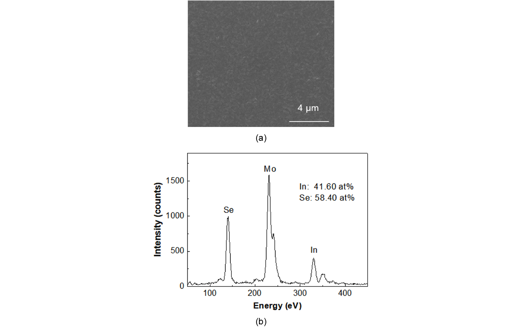
The SEM and EDS results were taken at 20 k and 10 k magnifications, respectively. The SEM image showed a flat surface without any pinhole or bump. From the EDS result, the compositions of In and Se were 41.6% and 58.4, respectively, and the film was slightly Se poor compared to the ideal case of In2Se3 (40% In and 60%Se). The Raman spectroscopy of the In2Se3 layer, not shown here, was well matched to the Raman spectroscopy data of γ-In2Se3 reported in literature21, 22).
Fig. 3 shows the optical transmittance and reflectance (a) and Tauc plot (b) of a 300-nm-thick In2Se3 film deposited at 300°C on a glass substrate. The transmittance of In2Se3 became monotonically lowered from 0.8 to 0.1 as the wavelength decreased from 800 to 600 nm. The reflectance of In2Se3 reached a maximum broad peak at 700 nm wavelength and minimum peaks at 600 and 820 nm due to thickness interference.
With the transmittance and reflectance data, the absorption coefficient was obtained. Then the band gap of In2Se3 was determined by absorption coefficient and Tauc plot in Fig. 3(b). The band gap of In2Se3 was measured to be 1.93 eV.
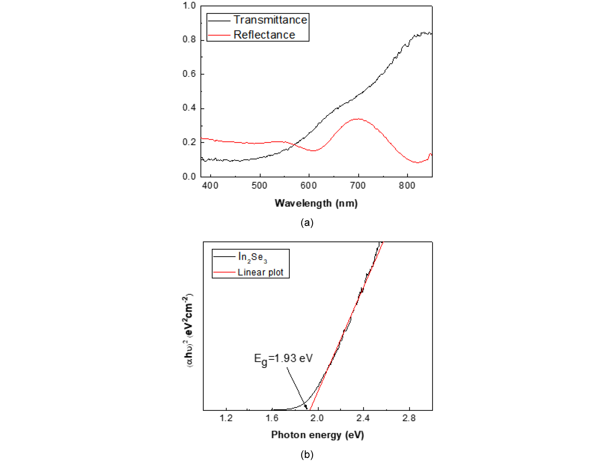
Fig. 4 showed the LTPL spectra of 300-nm-thick In2Se3 film deposited on Mo substrate, with various power densities for a 514-nm laser at 10 K. In the low excitation powers from 0.1 to 1 mW, two peaks (P1 at 2.13 eV and P2 at 2.11 eV) were observed. At 2.5 mW power, an additional weak peak with a low emission energy was observed at 2.05 eV. The peak intensity versus excitation power density can be given as
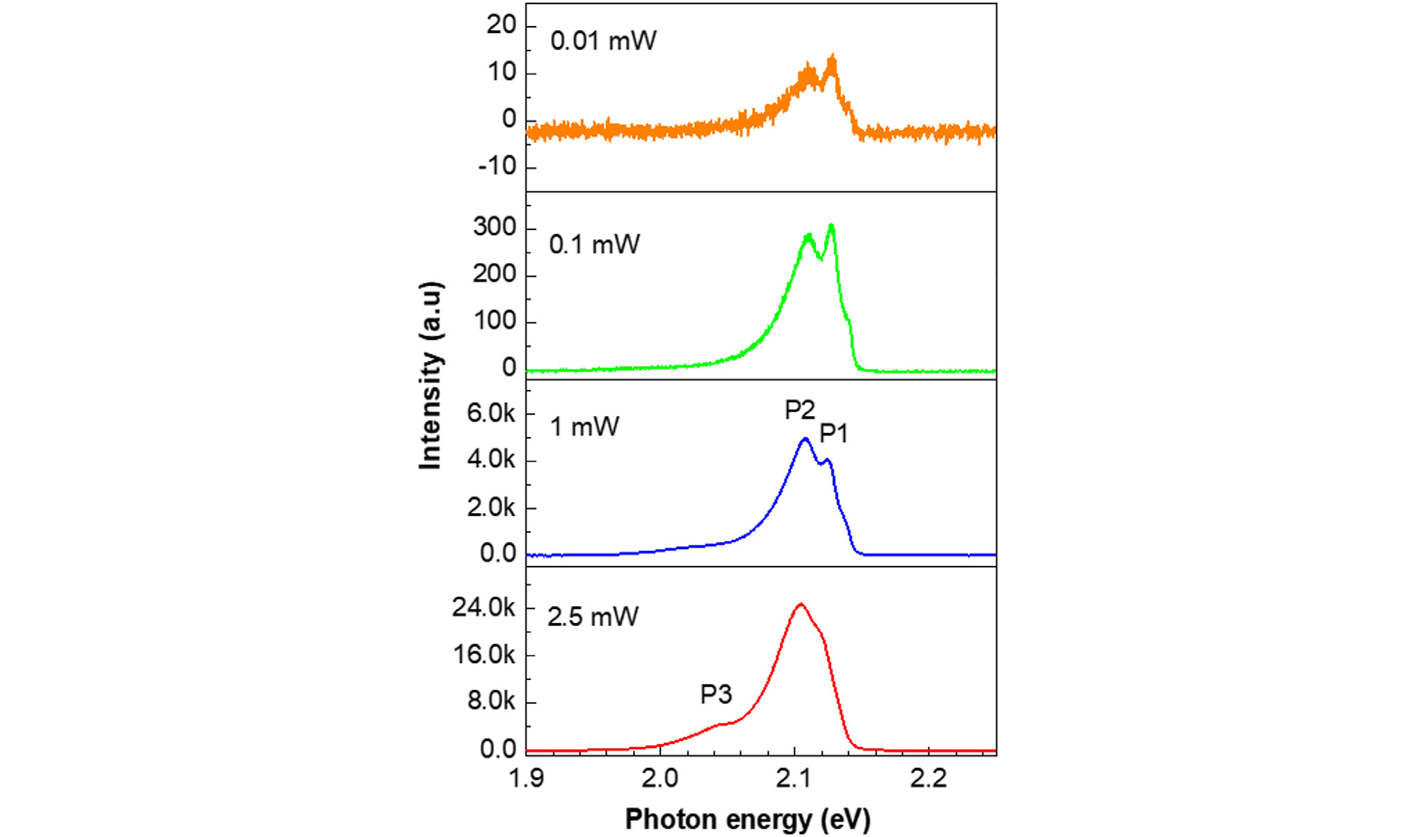
where pexc is the excitation power, IPL is the PL intensity at a specific excitation power, and k is the characteristic parameter for the emission peak.
The change of P1 peak intensity as a function of excitation power is shown in Fig. 5. From the log-log fitting of the data, the value of k was 1.3. The exciton is considered as a band-to-band transition for k > 1, and the exciton was considered as a free-to-bound transition or a donor-to-acceptor pair recombination for k < 123-25). This means that the P1 peak corresponds to band-to-band transition. The difference of photon energy between P1 and P2 is about 17 meV at 10 K.
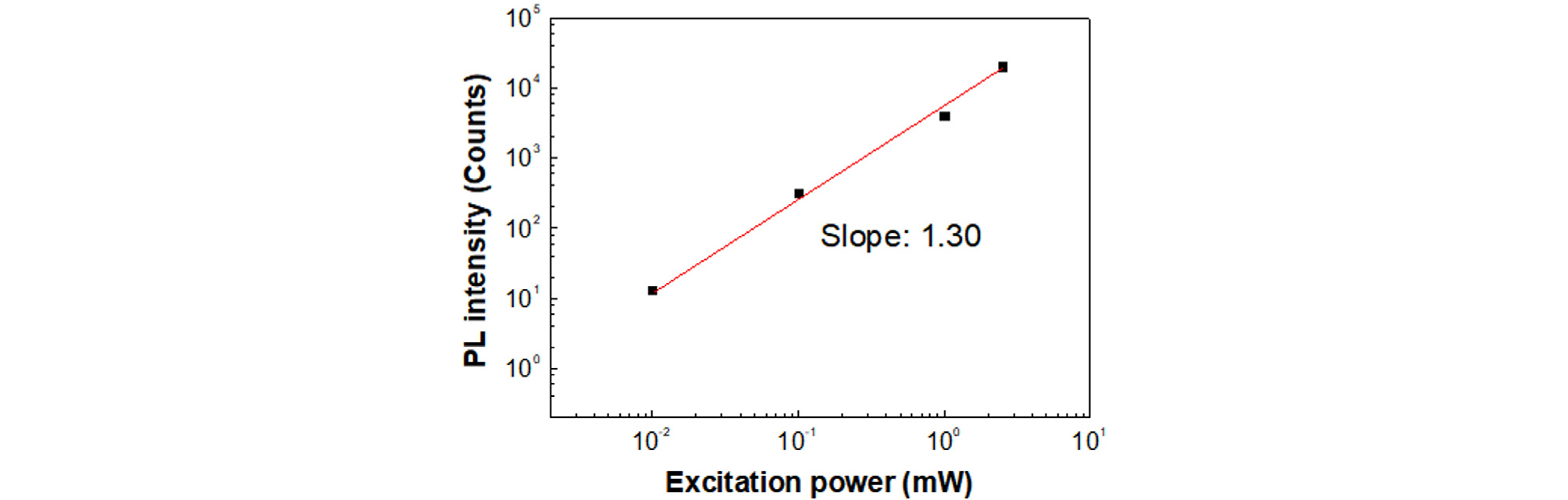
The ionization energy of selenium was about 40 meV, and the electron affinity of indium was about 38 meV. In addition, T. Ohtsuka et al. mentioned that the activation energy for bound exciton emissions of In2Se3 was greater than 22 meV26). Therefore, the P2 peak is expected to be a phonon replica of the P1 peak.
The P3 peak was located about 62 meV below the P2 peak or 79 meV below the P1 peak. Since the stoichiometry of the In2Se3 film deposited at 300°C in our experiment was Se poor, it was believed that the peak originated from the selenium vacancy with a very low concentration. The PL analysis signifies that the quality of In2Se3 film itself was good and the recombination In2Se3 film could be negligible.
3.2 Growth of In2Se3 on CIGS film
Unlike depositing an In2Se3 layer on glass or molybdenum substrate, upon growing an In2Se3 layer on CIGS film, there is a reaction between In2Se3 and the CIGS substrate due to the rapid out-diffusion of copper atoms from the CIGS substrate. The Cu diffusion into In2Se3 can form a CuInSe2 phase that has a lower band gap than CIGS, causing degradation of device performance.
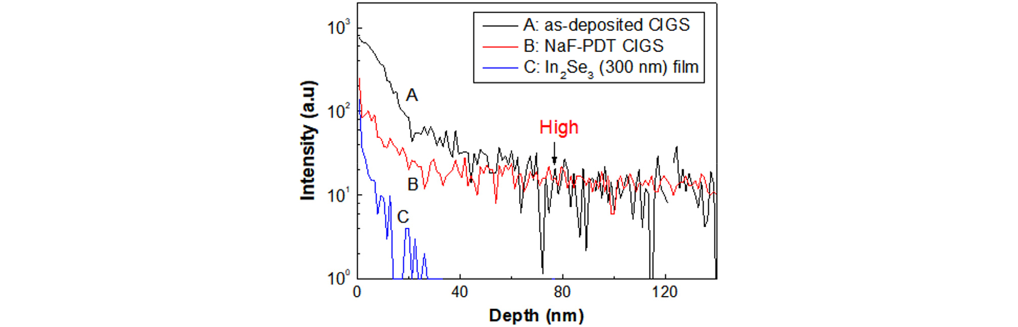
Fig. 6 shows the XPS depth profiles of Cu/(In+Ga) ratios in the as-deposited CIGS film prepared at 550°C by co-evaporation process and in the CIGS with NaF post-deposition-treatment (PDT) at 300°C17). This figure was taken to explain the Zn diffusion mechanism during the In2Se3 deposition. The Cu/(In+Ga) ratio on the surface of the as-deposited CIGS was 0.4, while that on the CIGS surface with NaF PDT was less than 0.2. With the NaF PDT process, the Cu/(In+Ga) ratio lowered substantially because Na alkali atoms occupy Cu sites and because Cu atoms were pushed away from the surface. Therefore, in case of CIGS film with alkali PDT, the out-diffusion of Cu from CIGS to In2Se3 film during In2Se3 growth could be greatly suppressed.
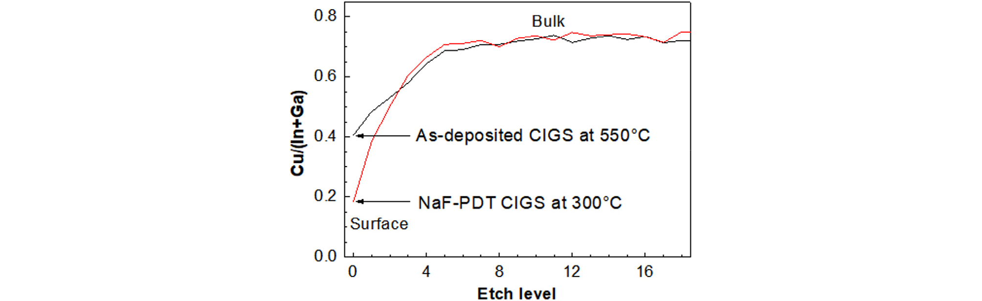
Fig. 6
AES depth profiles of Cu/(In+Ga) ratio in the as-deposited CIGS film at 550°C and NaF-PDT CIGS film at 300°C17)
To investigate a worst-case scenario or for possible elimination of the PDT process, an In2Se3 layer was grown on the as-deposited CIGS film at two different temperatures (300 and 400°C) by co-evaporating. Fig. 7 shows the Raman spectra of In-Se layers grown at 300°C and 400°C by supplying In and Se on as-deposited CIGS film and an in-Se layer grown at 300°C on a Mo substrate. The term In-Se layer means the layer grown by the ALD process but the phase is not defined correctly yet. The peaks of the In2Se3 phase and CIGS phase are located at 150 and 175 /cm, respectively, in Raman spectroscopy27, 28).
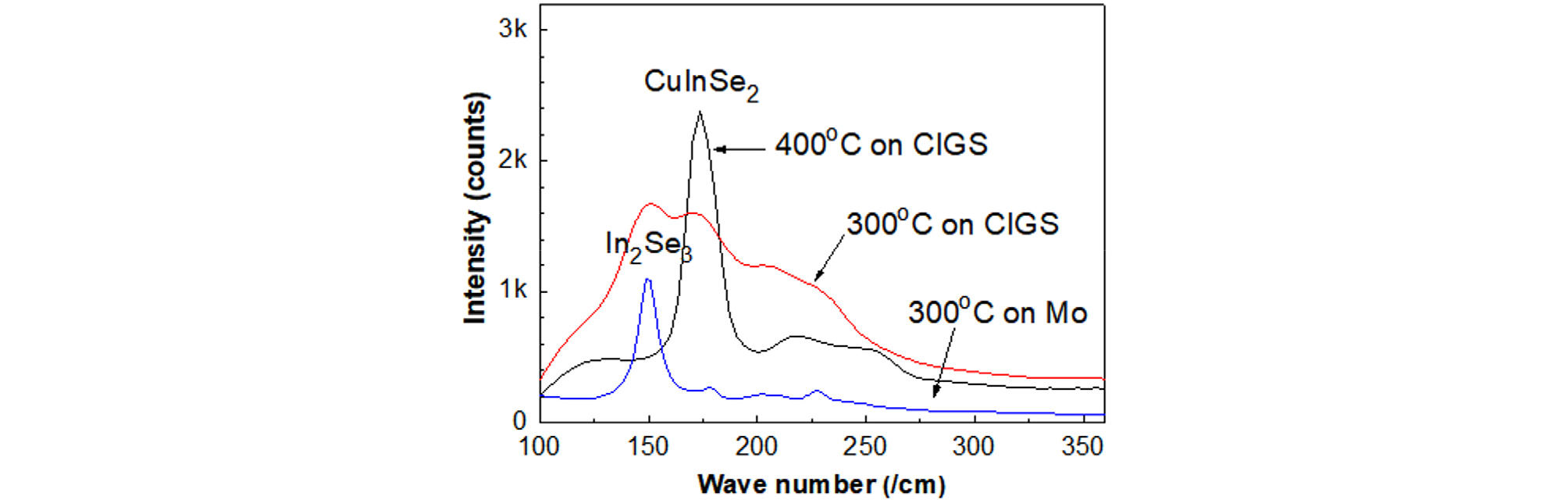
To detect photoelectron emission near the surface region, laser intensity was minimized by a laser filter just before the major peaks of CIGS and In2Se3. On the Mo substrate, a sharp In2Se3 peak was observed, indicating that an In2Se3 phase with a good crystallinity can be grown at 300°C. For the growth at 400°C on the CIGS substrate, only a CuInSe2 peak was observed, and no In2Se3 peak was observed, indicating that 400°C was too high of a temperature to grow an In2Se3 layer on a CIGS substrate. At 300°C growth on a CIGS substrate, both In2Se3 and CIGS peaks were observed.
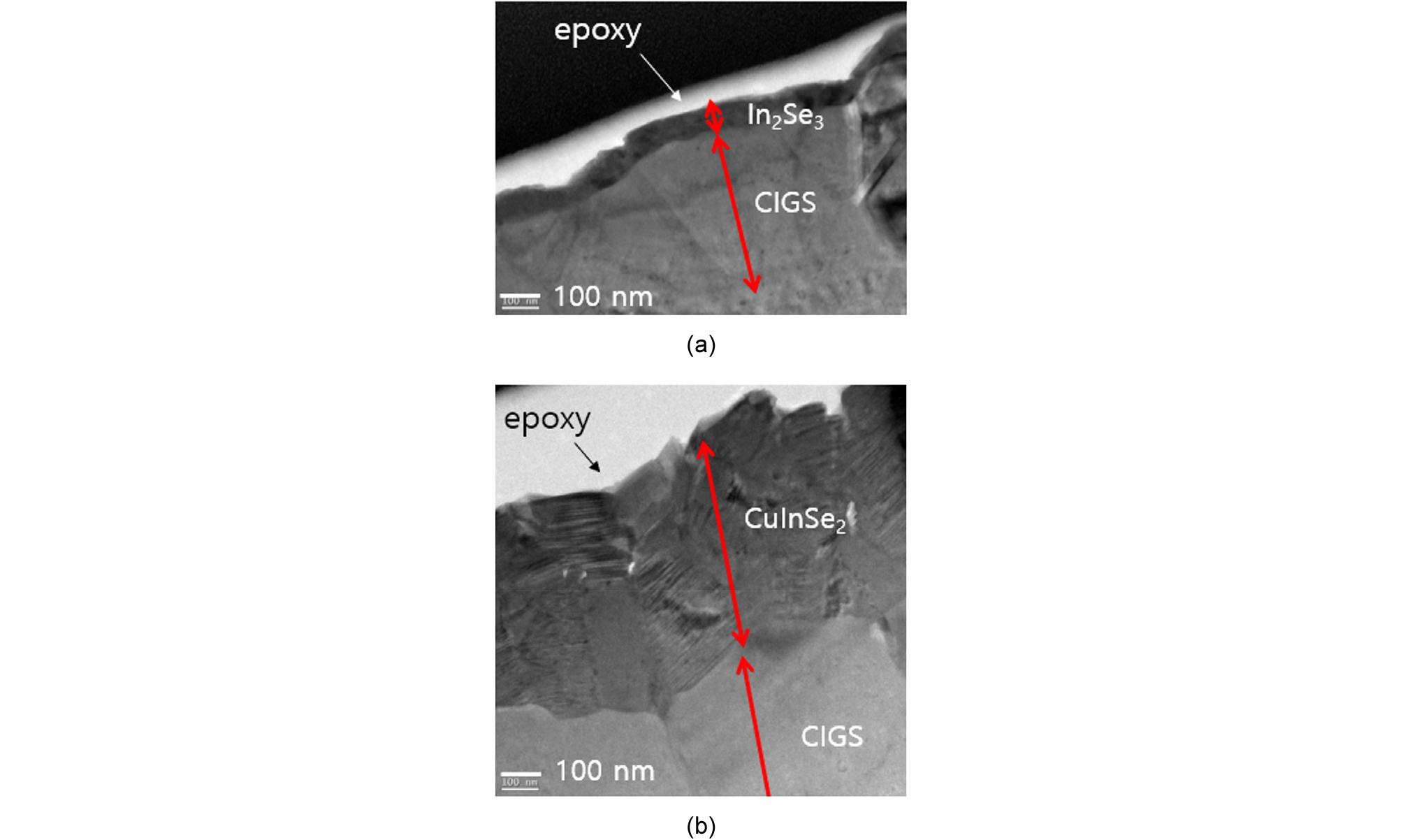
Fig. 8 shows TEM cross-sectional images of the In-Se layers grown at (a) 300°C and (b) 400°C on the as-deposited CIGS film that was prepared at 550°C. The film grown at 300°C for 30 min was around 50 nm. Since the thickness of In2Se3 grown at 300°C was very thin, the peak from the CIGS substrate was also observed. The film grown at 400°C for 30 min was CuInSe2 phase with more than 300-nm thickness, which was validated by Raman spectroscopy.
To further confirm the compositions in those layers, EDS composition analysis was conducted both In2Se3/CIGS interface and CuInSe2/CIGS interface. Fig. 9 shows the cross-sectional EDS analysis of the In2Se3/CIGS film, where the In2Se3 layer was grown at 300°C by supplying In and Se on as-deposited CIGS film. In the In2Se3 region, the Ga and Cu intensities were negligible, while the In intensity was very high. From the Cu, Ga, and In distribution, the demarcation between In2Se3 and CIGS was clearly shown. Therefore, it was considered that the 50-nm-thick layer on the CIGS surface was In2Se3 phase. The EDS image could not exclude the existence of Cui and Ga as solid solution.
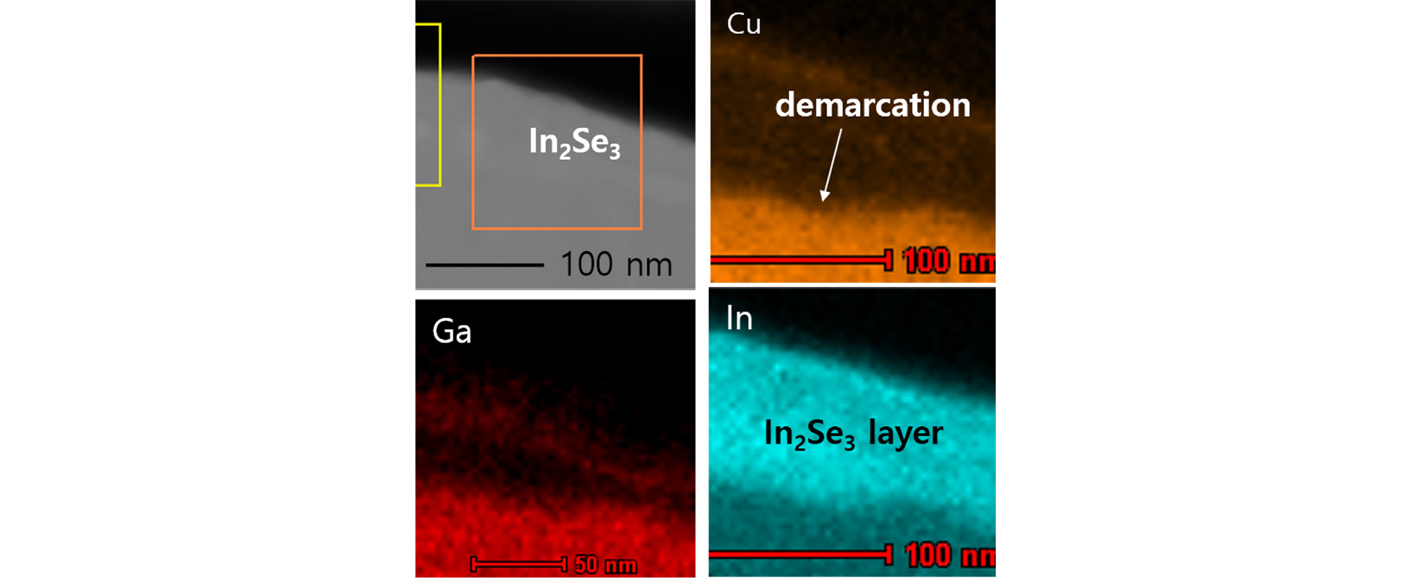
Fig. 10 shows the cross-sectional EDS analysis of CuInSe2/CIGS film, where the CuInSe2 layer was grown at 400°C by supplying In and Se on CIGS film. The images shown in Fig. 10 cover CuInSe2 phase with a thick layer (>300 nm). In the CuInSe2 region, the Ga intensity was negligible, while both the Cu and In intensities were very high. This indicates that Cu atoms were diffused out and Ga atoms were not diffused out from the CIGS surface at 400°C process.
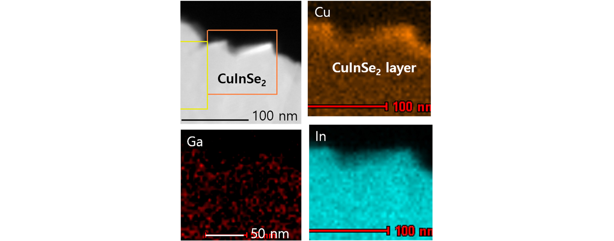
Fig. 11 shows the XPS depth spectra of Cu 2p3/2 on the In2Se3 surface layer (a) and on the CuInSe2 surface layer (b). The In2Se3 and CuInSe2 layers were grown at 300°C and 400°C, respectively, by supplying In and Se on the as-deposited CIGS film.
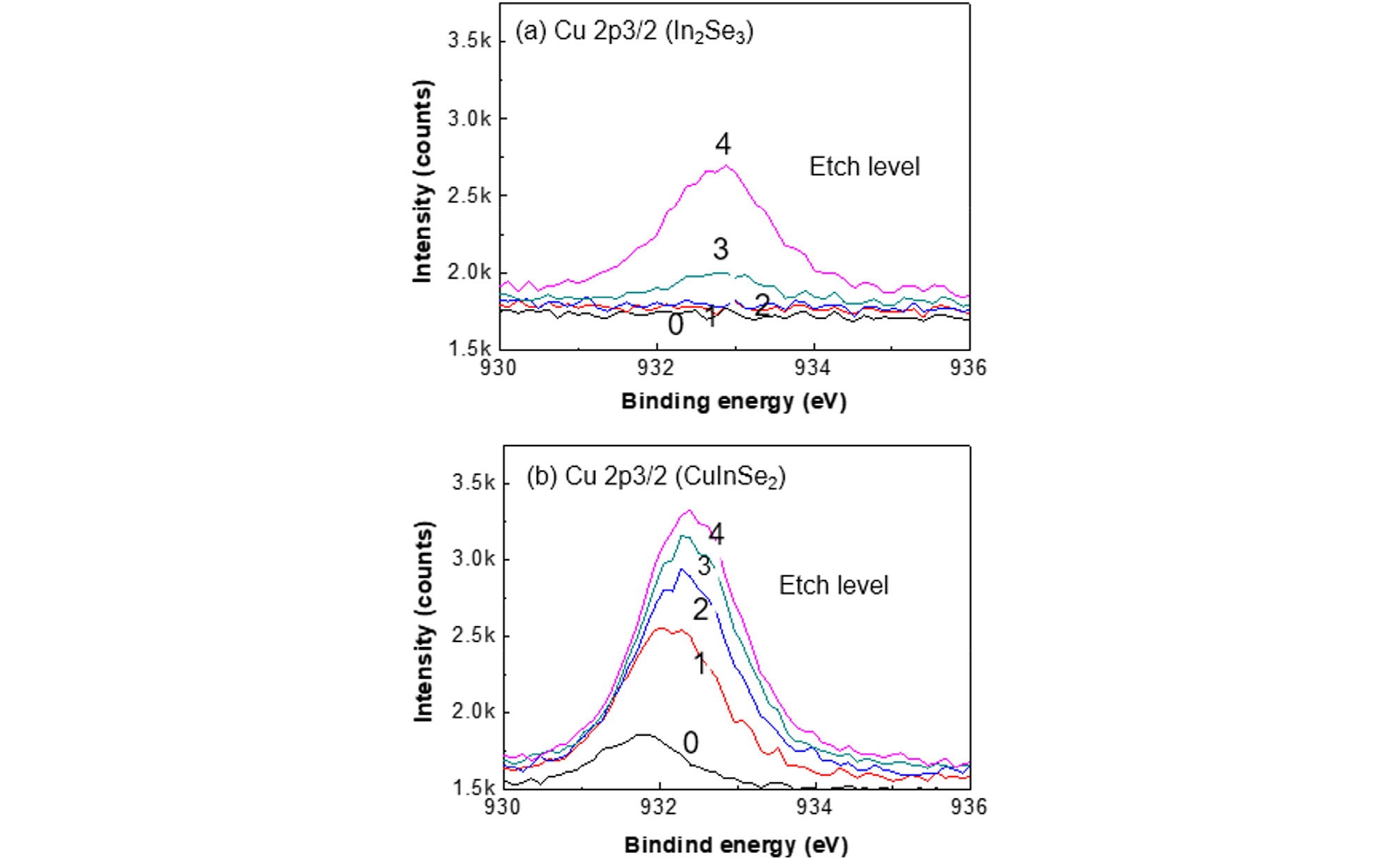
In the case of 300oC growth, a copper peak was not detected in the In2Se3 layer for 1st and 2nd etch levels and barely detected at the 3rd etch level. From EDS analysis the existence of Cu and Ga was not negligible. But, From the XPS analysis it was seen that Cu was excluded from the top surface. This confirms that a pure In2Se3 formed at 300°C growth at the CIGS surface up to 2nd level. Since the resolution of XPS is around 1%, pure In2Se3 means the Cu content is below 1%.
The Cu detected in the fourth etch level could be the originated from the substrate CIGS film. The demarcation between In2Se3 and CIGS was not clear in the XPS depth profile due to interface roughness. In the case of 400°C growth, copper was detected from the surface of CuInSe2 layer and throughout the CuInSe2 film, confirming that CuInSe2 surface layer exists.
From the Raman spectroscopy, TEM images, EDS analysis, and XPS analysis, it was confirmed that a pure In2Se3 layer could be grown at 300°C on as-deposited CIGS film. Since the Cu/(In+Ga) ratio on the surface of CIGS film with an alkali PDT process is about one-half of the ratio on the as-deposited CIGS film, growing a pure In2Se3 layer at 300°C is much more likely.
3.3 Zinc suppression in CIGS interface with an In2Se3 layer
As we mentioned in the Introduction section, in CIGS, zinc atoms can easily move from buffer layer to CIGS through copper vacancies sites in the CIGS film because the CIGS film used for solar cell application has a Cu-poor stoichiometry. To determine the diffusion length of zinc in In2Se3 and CIGS films, a ZnSnO buffer layer was deposited on an In2Se3 film and on a CIGS film by the ALD process, which was described in the experimental section. The 300-nm thick In2Se3 film was grown at 300°C on the as-deposited CIGS film.
Fig. 12 shows the SIMS depth profiles of zinc atoms on the surfaces of the as-deposited CIGS film, NaF-PDT CIGS film, and In2Se3 film. The as-deposited CIGS film was prepared at 550°C, and the NaF PDT process was conducted at 300°C19). A ZnSnO buffer layer was deposited on these films at 300°C for 30 min by an ALD process and was etched off with an HCl solution to avoid the knock-on effect during the SIMS depth profile. With the chemical etching, only oxide was removed and selenide was not etched20).
On the as-deposited CIGS film, the Zn concentration at the CIGS surface was high, and zinc atoms penetrated above 100 nm from the CIGS surface. On the NaF-PDT CIGS film, the intensity of Zn at the surface was one order of magnitude lower than that on the as-deposited CIGS film. The reason of low Zn intensity at the surface with NaF PDT is due to no available Cu vacancy sites by Na occupation by NaF PDT. Zn atoms can easily diffuse through interstitial sites. However, the Zn intensity in the 50- to 120-nm depth was similar to that of as-deposited CIGS film. This indicates that the Zn concentration at the CIGS surface can be greatly reduced at the surface but that, in the subsurface, the Zn concentration is not negligible. On the In2Se3 film, the intensity of Zn at the surface was one order of magnitude lower than that of as-deposited CIGS film and similar to that of NaF-PDT CIGS film. It was noted that the Zn intensity was rapidly diminished in the case of depth less than 30 nm. In this case, the Zn intensity at 20-nm depth was one-tenth lower than that of the base intensity in CIGS film. This indicates clearly that In2Se3 film is a highly effective barrier material for Zn diffusion.
By using the data from Fig. 12 and the general solution for Fick’s second law,
the relative values of diffusion coefficient were calculated. The zinc diffusion coefficient ratio, in as-deposited CIGS and in In2Se3, DZn(CIGS)/DZn(In2Se3), was about 11. Again, our result showed that In2Se3 layer can have a major advantage as a Zn diffusion barrier for a CIGS absorber that adopts Cd-free ALD buffers containing Zn.
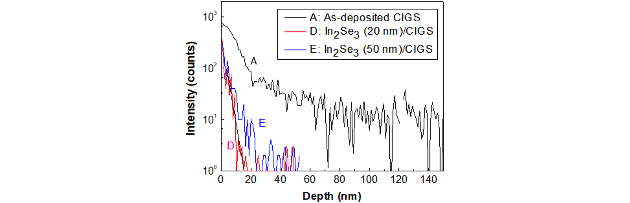
Fig. 13 shows the SIMS depth profile of Zn atoms in the as-deposited CIGS films with or without an In2Se3 passivation layer. An ALD ZnSnO buffer was deposited at 120°C for 30 min on these films and chemically etched off before depth analysis. 20-nm-thick and 50-nm-thick In2Se3 layer were deposited on the CIGS absorber layer to verify the thickness effect of the In2Se3 layer.
The SIMS intensity of Zn atoms was sharply diminished with the In2Se3 passivation layer, and the base intensity throughout the CIGS film in the In2Se3/CIGS structures was again one order of magnitude smaller. Therefore, the In2Se3 layers with both 20-nm and 50-nm thicknesses performed well as a diffusion barrier of zinc atoms from ALD ZnSnO buffer to CIGS absorber.
The depth profile of Zn atoms with a 20-nm-thick In2Se3 layer was similar as that of Zn atoms with 50-nm thickness in Fig. 13. A thinner In2Se3 film can have advantages with less series resistance, less light scattering, and short process time. Since controlling the thickness of In2Se3 below 20 nm was difficult in practice in our co-evaporation process, it seemed that a 20-nm-thick In2Se3 layer was the optimum condition as a Zn diffusion barrier at the ALD ZnSnO/CIGS interface.
3.4 Band structure of In2Se3/CIGS film
Fig. 14 shows the XPS valance-band spectra at the surfaces of the as-deposited CIGS film prepared at 550°C, of the NaF-PDT CIGS film processed at 300°C, and of the In2Se3 film grown at 300°C on the as-deposited CIGS substrate. The valence band maximum (VBM) of each film can be determined by the extrapolation of maximum slope from the spectra. The VBM values of the as-deposited CIGS, NaF-PDT CIGS, and In2Se3 were -0.4. -0.52, and -1.2 eV, respectively, from the Fermi level.
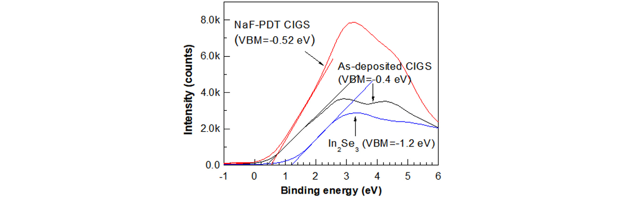
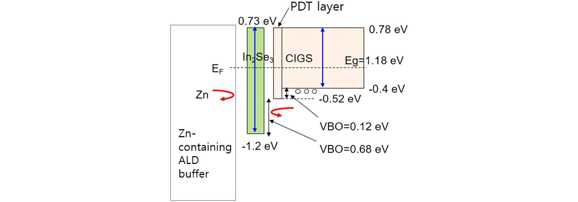
Fig. 15 shows the electronic band structure of In2Se3/CIGS interface after the NaF-PDT process, constructed based on the XPS results and optical measurement. Valence band offset (VBO) is the VBM difference between two different regions or materials. The VBO value between the CIGS surface after NaF PDT and the CIGS surface of the as-deposited CIGS was 0.12 eV. The VBM lowering by NaF PDT, named as PDT layer, serves as a hole-blocking layer17). The VBO value between the In2Se3 layer and NaF-PDT CIGS surface was 0.68 eV, which was five times larger than 0.12 eV. Therefore, the In2Se3 layer can be a good candidate as for hole-blocking layer. Based on the excellent barrier for Zn diffusion during Zn-containing ALD buffer and good band alignment at the In2Se3/CIGS surface, it is expected that the insertion of an In2Se3 layer can be an excellent passivation layer for CIGS solar cells that consist of Cd-free ALD buffers containing Zn and can have serious potential to achieve super-high-efficiency Cd-free CIGS solar cells. Device fabrication with In2Se3 buffer is beyond the scope of this paper.
4. Conclusions
Due to the Zn diffusion from Zn-containing ALD buffers into CIGS film during the ALD process of growing a buffer layer, the cell performance of the CIGS solar cell was degraded. To prevent Zn diffusion, an In2Se3 layer that has no Zn component was characterized as having potential use as a passivation layer at the Zn-containing ALD buffer/CIGS interface. The In2Se3 film grown at 300°C by co-evaporating In and Se elements showed a Se-poor stoichiometry with a band gap of 1.93 eV. A Se-vacancy-related defect was barely detected in the LTPL spectrum at a high excitation energy of 2.5 mW.
Growth of In2Se3 film on the CIGS substrate was greatly affected by the growth temperature. At 400°C, CuInSe2 phase was grown instead of In2Se3 because Cu atoms were diffused out to the In2Se3 layer. At 300°C, a pure In2Se3 phase was grown, indicating that an In2Se3 layer should be grown at or below 300°C. Raman spectra, TEM images, EDS analysis, and XPS analysis confirmed that a thin In2Se3 with no Cu can be grown at 300°C on a CIGS substrate by co-evaporating In and Se.
With ALD ZnSnO process at 120°C for 30 min, the diffusion of Zn atoms into the In2Se3 layer was limited to about 20 nm, while that into CIGS film was more than 100 nm. Of note, the SIMS base intensity of Zn atoms in In2Se3 film was one order of magnitude lower than that in CIGS film, where Zn diffused rapidly through Cu-vacancy sites in the CIGS film. The 20-nm-thick In2Se3 layer in the ZnSnO/In2Se3/CIGS structure demonstrated that Zn diffusion into CIGS film can be effectively prevented.
The VBO value between In2Se3 layer and the CIGS surface after NaF-PDT was 0.68 eV, while the value between the CIGS surface after NaF PDT and the CIGS surface for as-deposited film was 0.12 eV. It suggests that the In2Se3 can serve as an effective hole-blocking layer.
Based on its excellent diffusion barrier of Zn atoms from Zn-containing ALD buffer and good band alignment with large VBO at the In2Se3/CIGS interface, it is expected that the insertion of an In2Se3 layer deposited at or just below 300°C can be an excellent passivation layer for CIGS solar cells and can lead to a super-high efficiency in Cd-free CIGS solar cells. Device fabrication with In2Se3 buffer is beyond the scope of this paper.
