

1. Introduction
2. Experimental
3. Results and Discussion
3.1 Morphologies in CZTSSe films
3.2 Phase evolution in the S-S annealing
3.3 Phase evolution in the N-S annealing
3.4 Device performance
4. Conclusions
1. Introduction
For many years, kesterite-based materials including Cu2ZnS4 (CZTS), Cu2ZnSe4 (CZTSe), and Cu2ZnSn(S,Se)4 (CZTSSe) have been considered as promising absorbers for thin film solar cells because of its abundance of raw materials on the earth and their low prices. The record power conversion efficiencies (PCE) of CZTS, CZTSe, and CZTSSe are 11.0%, 12.5%, and 12.6%, respectively1-3), which are well below the theoretical efficiency of 32% yet4,5). Even though the current efficiencies are low, consistent attention is necessary for these material because of very attractive candidate for future generation of low-cost solar cell.
In the solar cells based on these materials, the open-circuit voltage (Voc) gain and fill factor (FF) are especially low compared to high-performance solar cells, which are the bottleneck in efficiency enhancement. The Voc gain, which is the ratio of Voc to band gap Eg, is below 60% and the FF is below 70% in kesterite-material solar cells6). The main reason for such low Voc gain is the existence of point defects in the CZTS film7). One of the basic ways to increase Voc is to adjust the band gap of the light-absorbing material to 1.4 eV8). The band gaps of CZTSe and CZTS are 0.96 and 1.5 eV, respectively, and the band gap of CZTSSe can be tuned between the two values with an appropriate mixing of Se and S during the CZTSSe film growth.
To grow a CZTSSe thin film with Se-S solid solution, various techniques including solution process3,9,10), co-evaporation11), sputtering and sulfurization12), sputtering and sulfo-selenization of metal precursor13-15), and spray deposition16) have been employed. Apparently the solution growth process seemed most effective. However, for large-area application, sputtering of metallic Cu/Zn/Sn precursor followed by sulfo-selenization process seems a good approach. More details on the fabrication technics and device structures can be found in the recent review papers17,18).
In the sulfurization of sputtered metal precursor, large volume expansion can cause a lift-off phenomenon. As a result, the PCE of the cell ranged from 3.17% to 12.63%, depending on the sulfurization or selenization process12-15).
We also observed a severe lift-off during sulfurization with the PCE was around 5%12). The adhesion problem by the volume expansion can be relaxed by introducing Se or S into the metal precursor. For example, a precursor that contains Se in the form of Cu/SnSe2/ZnSe precursor resulted in no lift-off of the CZTSe film19).
To increase open-circuit voltage, it is necessary to insert S into the CZTSe film. For the purpose, the Cu/SnSe2/ZnSe precursor was sulfurized in sulfur environment. However, direct sulfurization of Cu/SnSe2/ZnSe precursor at 550°C resulted in non-uniform CZTSSe film as shown in Fig. 1. A large-area lift-off spot can be observed in the dashed circle area due to uneven reaction and uneven local thermal stress.

In order to obtain a uniform CZTSSe film, we introduced a pre-annealing stage in S or N2 below 400°C before post-annealing at 550°C. The morphology and growth mechanism of CZTSSe film with the two different pre-annealing were investigated.
2. Experimental
The Cu/SnSe2/ZnSe precursor was prepared by sputtering of Cu, SnSe2 and ZnSe targets on a Mo-coated sodalime-glass substrate. The Cu was deposited by DC sputtering and the selenides were deposited by RF sputtering. The sputtering powers used for Cu, SnSe2, and ZnSe were 80, 60, and 50 W, respectively, in 1 mTorr working pressure.
The cross-sectional scanning electron microscope (SEM) image of the precursor is shown in Fig. 2(a). The thicknesses of Cu, SnSe2, and ZnSe were around 0.1, 1, and 1 μm, respectively. The SnSe2 and ZnSe layer showed columnar morphologies which were a typical morphology by sputter deposition.
Then the as-deposited precursors contained in a graphite box were pre-annealed below 400°C for 10 min and post-annealed at 550°C for 5 min with two different pre-annealing environments: S and N2. The schematic of temperature profile is shown in Fig. 2(b). The process with S pre-annealing and S post annealing was denoted as ‘S-S annealing’ and that with N2 pre-annealing and S post-annealing was denoted as ‘N-S annealing’.
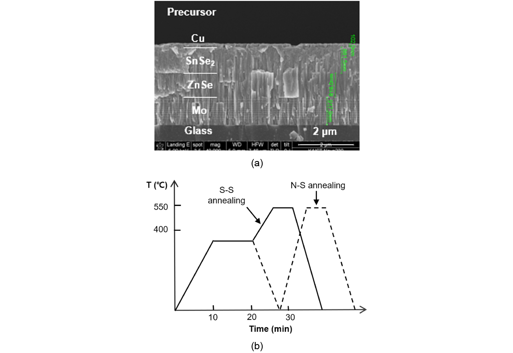
The main difference between the two process was S charging sequence into a carbon crucible that contained precursor sample. In the S-S annealing, the S powder was charged into the carbon crucible that contained precursor film. The crucible was pre-annealed in a in a closed quartz tube filled with 1-atmosphere Ar gas. There was no tube opening in the S-S annealing. In the N-S annealing, a carbon crucible that contained precursor was pre-annealed in the closed quartz tube that filled with 1-atmosphere N2. After the N2 pre-annealing, S powder was charged at room temperature and then post-annealed in the quartz tube filled with 1 atmosphere Ar gas.
The phases existing after pre-annealing and post-annealing were identified with x-ray diffraction (XRD) studies using Rigkagu Optima IV X-ray diffractometer with Cu Kα (λ =1.5416Å) source at 30 kV and 60 mA. The existing phases were also identified with Raman spectroscopic measurements using the Raman (Horiba Jobin Yvon ARAMIS) spectroscopy source with 514 nm emission line of Ar ion laser. The surface and cross-sectional morphologies of the films were examined with field-emission scanning electron microscopy (FE-SEM, FEI Nova230). The composition of the films was determined with energy dispersive spectroscopy (EDAX) with 20 kV attached to the FE-SEM. Auger depth profile of a film carried out using Auger emission spectroscopy (Perkin Elmer SAM4300).
3. Results and Discussion
3.1 Morphologies in CZTSSe films
Fig. 3 shows the SEM surface images of CZTSSe films fabricated by the S-S annealing: S pre-annealing and S post-annealing. S200-S550, S300-S550, and S400-S550 were denoted for S pre-annealing at 200, 300, and 400°C and S post-annealing at 550°C, respectively. In the S200-S550 film, equiaxial grains with gain facets were densely connected. However, the extrusion of grains from surface and deep valleys between grains indicated that the surface was not appropriate for further coating of a 70-nm thin CdS buffer layer.
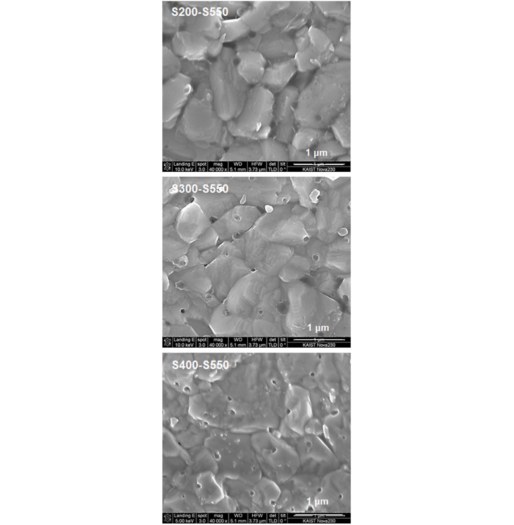
In the S300-S550 film, the grain boundaries were more densely connect with more round-shaped grains and smoother surface was observed compared to S200-S500 surface. In the S400-S550 film, grains were not well defined and surface were smoother than S300-S550 surface.
It was noted that small pinholes with less than 10-nm diameter were observed at the surface. The number of the small pinhole increased as the S pre-annealing temperature increased. The shape of the pinholes was similar to that of volcano mouth. The origin of the pinholes might be the evolution of a Se gas phase at high-temperature post-annealing stage along with rapid grain growth. The volcano mouths were distributed in random locations in S400-S550 sample.
Fig. 4 shows the surface image of the CZTSSe films fabricated by the N-S annealing: N200-S550, N300-S550, and N400-S550 were denoted for N2 pre-annealing at 200, 300, and 400°C and S post-annealing at 550°C, respectively. In the N200-S550 film, small grains with faceted plate-shaped grains were observed on the film surface. The surface was too rough with too much free volume so that subsequent thin film coating on the surface was not possible.
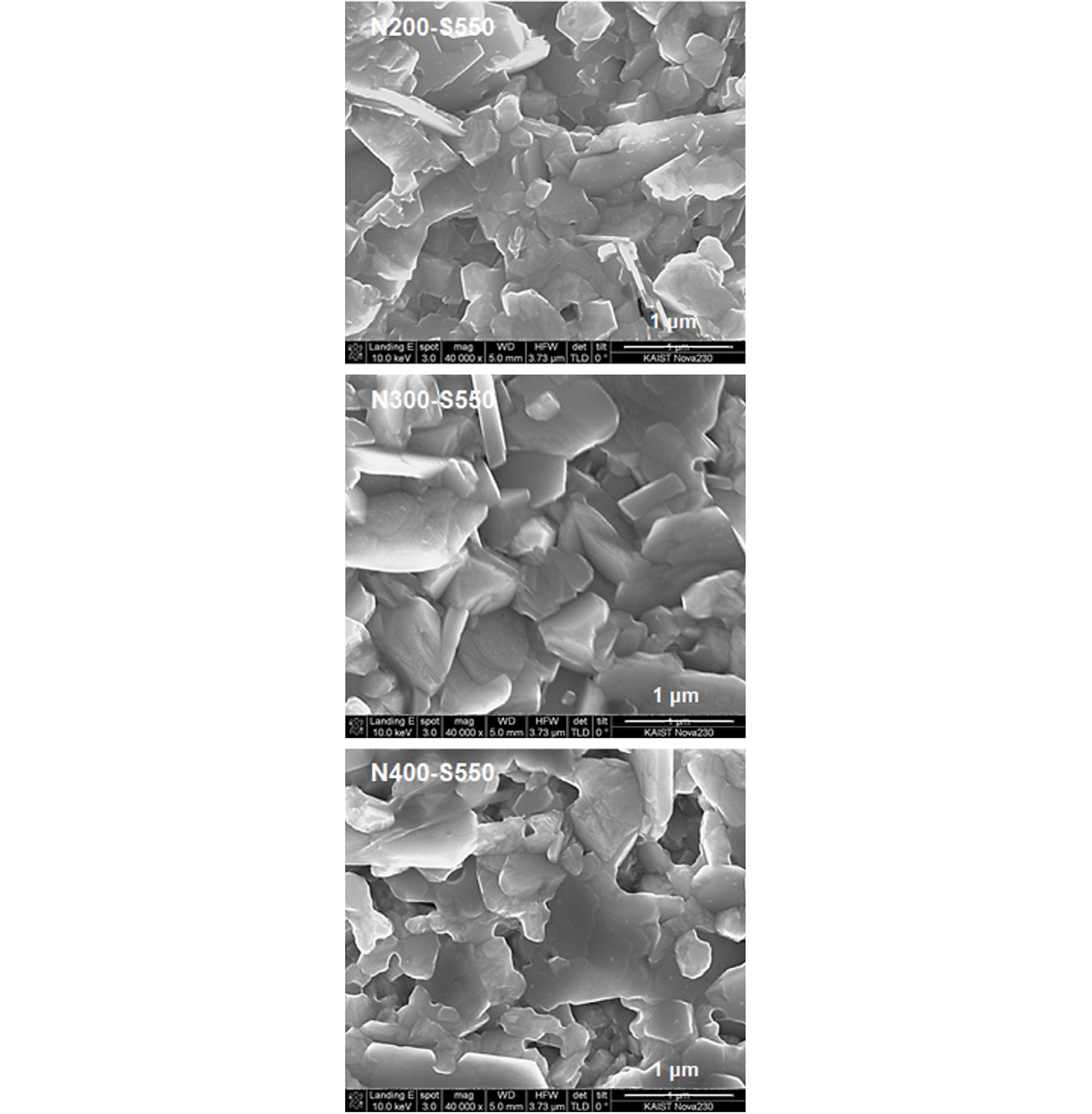
In the N300-S550 film, the plate-shaped grains were well faceted and well developed to around 1 μm. In the N400-S550 film, the edge of the plate-shaped grains became mushier or lost facet. In the N400-S550 film, grains lost their facet due to active migration of its component at higher temperature.
In overall, the surface morphology the CZTSSe film prepared by the N-S process showed that the N-S process was not appropriate for thin-film application because of its extreme rough surface and too many voids in in the CZTSSe layer.
Fig. 5 shows the cross-sectional SEM images of the CZTSSe films prepared by the S-S annealing and N-S annealing, denoted as S300-S550 and N300-S550 in Fig. 3 and Fig. 4, respectively. In the S300-S550 film, grains with around 1-μm diameter were densely connected among them. A small-grained Zn(S,Se) layer was observed between the CZTSSe layer and Mo substrate. The thickness of CZTSSe and Zn(S,Se) layers were 1 μm and 250 nm, respectively. The thickness of the Zn(S,Se) layer can be reduced by reducing the thickness of ZnSe precursor layer. However, thickness and composition control of the Zn(S,Se) layer might be a challenging issue because of its uniformity variation at the CZTSSe/Mo interface.
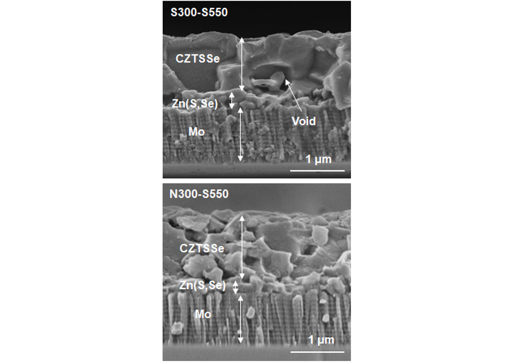
It was also noted that one large void with 500-nm diameter was observed at the CZTSSe/Zn(S,Se) interface. Other than the one large void, the film prepared by S300-S550 anneal seem appropriate for subsequent coating of 70-nm thick CdS buffer layer on it.
In the N300-S550 film, grains were not closely packed together and many voids and crevices were observed among grains. The thickness of the CZTSSe was around 1.3 μm and that of the Zn(S,Se) layer was around 100 nm, resulting in a thicker CZTSSe layer and thinner Zn(S,Se) layer. The thinner Zn(S,Se) layer compared to that in the S-S annealing indicated that the sulfurization reaction was more aggressive in the N-S annealing than in the S-S annealing. Since the surface of the film prepared by the N-S annealing was very rough and the bulk of the film was so much porous, the N-S annealing seemed not appropriate for thin-film device application.
The compositions of the films shown in Fig. 3 and Fig. 4 were analyzed by AES were listed in Table 1. In the S-S annealing, the S/(S+Se) ratio decreased from 0.64 to 0.25 as the S pre-annealing temperature increased from 200 to 400°C. In the N-S annealing, the S/(S+Se) ratio decreased from 0.90 to 0.78 as the N2 pre-annealing temperature increased from 200 to 400°C. Two notable results were observed in Table 1: big difference in the ratio between the S-S annealing and the N-S annealing and gradual change with the pre-annealing temperature within the same process.
The results could be explained by considering the charging sequence of S powder into the graphite box and amount of S loss from the graphite box. S powder was charged into the graphite box before pre-annealing in the S-S annealing, while S powder was charged into the graphite box after N2 pre-annealing of precursor in the N-S annealing.
In the S-S process, the supply of S into precursor was limited by the CuS layer and by the remaining S in the graphite box. Somehow, the amount of remaining S in the graphite would be smaller due to more leak between graphite cap and holder due to higher S pressure. Aa s result, the total S amount that provided to CZTSe film decreased as the S pre-annealing temperature increased.
In the N-S process, the amount of S provided at the S post annealing was the same. In this case, the phases formed in the high-temperature N2 pre-annealing were less reactive than those formed in the low-temperature N2 pre-annealing. The unreacted excess S could be released from the graphite box. Therefore, the total amount of S that provided to CZTSSe film decreased as the N2 pre-annealing temperature increased.
The S/(S+Se) ratio by the N-S annealing was much larger (0.78 to 0.90) than that by the S-S annealing (0.25 to 0.64). This was due to fast and rigorous reaction between S and the pre-annealed precursor film at high temperature (550°C) with much less loss of S leak. Since the S/(S+Se) ratio ranged from 0.23 to 0.64 in the S-S annealing, it was seen that the ratio could be easily controlled by simply controlling the S pre-annealing temperature.
Fig. 6 shows the AES depth profiles of Cu, Zn, Sn, Mo, S, and Se elements through the CZTSSe film prepared by the S300-S550 annealing with the cross-sectional morphology shown in Fig. 5. The Cu, Zn, Sn, S, and Se content were uniformly distributed up to 1 mm depth. In the zone, the concentrations of Cu, Zn, Sn, S, and Se were 19.0, 14.5, 12.1, 23.2, and 26.0%, respectively. The calculated stoichiometry in the CZTSSe zone corresponded Cu1.57Zn1.20SnS1.92Se2.15. The S/(S+Se) ratio in the CZTSSe zone was around 0.47, which was smaller than bulk value of 0.53 listed in Table 1. This was due to the exclusion of S in the Z(S,Se) layer. value in Table 1 was due to A Zn(S,Se) layer that contains more S.
In Fig. 6, a Zn(S,Se) layer with a thickness of around 200 nm was observed between the CZTSSe and Mo substrate. In the region, the concentrations of Zn, S, and Se at the 1.1-mm depth were 28, 36, and 28, respectively. The S/(S+Se) at the 1.1-mm depth was around 0.56. The S concentration in the Zn(S,Se) region is higher than that in the CZTSSe region. The thickness of the Zn(S,Se) region can be further reduced by reducing the ZnSe thickness in precursor.
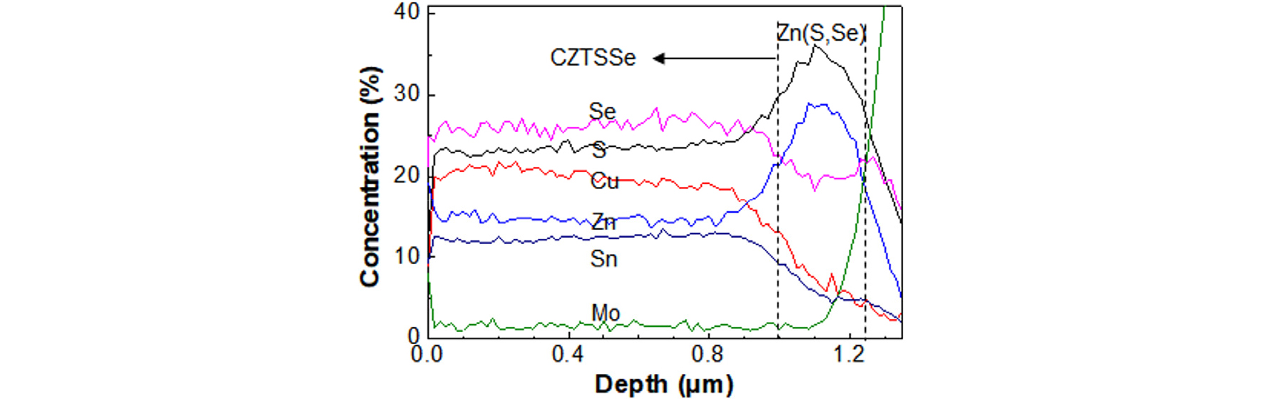
Fig. 6
AES depth profiles of Cu, Zn, Sn, S, Se, and Mo elements through the CZTSSe film prepared by the S300-S550 annealing with the cross-sectional morphology shown in Fig. 5
Table 1.
AES compositions in the CZTSSe films after two-stage annealing
| Annealing | Cu/(Zn+Sn) | Zn/(Zn+Sn) | S/(S+Se) |
| S200-S550 | 0.83 | 0.53 | 0.64 |
| S300-S550 | 0.85 | 0.55 | 0.53 |
| S400-S550 | 0.73 | 0.50 | 0.25 |
| N200-S550 | 0.71 | 0.53 | 0.90 |
| N300-S550 | 0.71 | 0.51 | 0.84 |
| N400-S550 | 0.74 | 0.49 | 0.78 |
3.2 Phase evolution in the S-S annealing
Fig. 7 shows the XRD patterns of the as-deposited precursor film, S pre-annealed films, and S-S processed films. S100, S200, S300, and S400 denoted for the samples with S pre-annealing at 200, 300, and 400°C for 10 min and S200-S550, S300-S550, and S400-S550 denoted for the samples with after S post-annealing at 550°C for 5 min in addition to S pre-annealing at various temperatures.
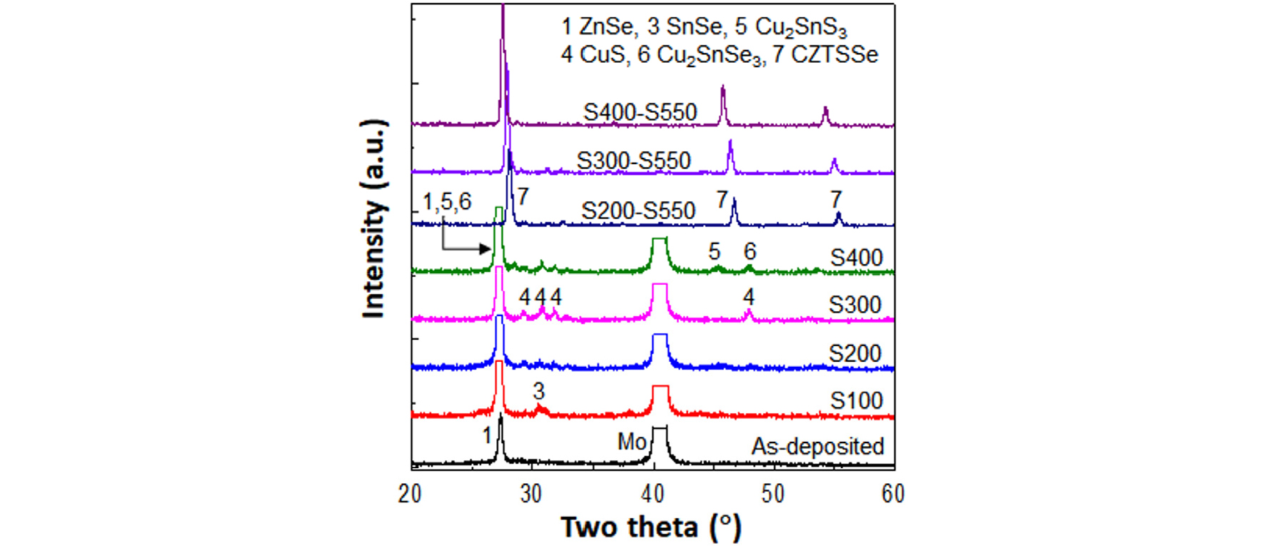
In the as-deposited film, only ZnSe peak (JCPDF #37-1463) was observed because the Cu in the precursor was too thin and the SnSe2 in the precursor was an amorphous state. At 100°C, SnSe peak was observed by partial crystallization of the amorphous SnSe2 layer. At 200°C, the peaks corresponding to CuS (PDF # 65-3588) phases appeared, indicating that Cu on the top surface was sulfurized. At 300°C, the CuS peaks were clearer than those at 200°C. At 400°C, ternary phase representing cubic Cu2SnS3 and spharelite Cu2SnSe3 were observed21,22).
After S-S annealing (S200-S550, S300-S550, and S400-S550 samples), only CZTSSe peaks were observed. The peak of the remaining Zn(S,Se) might be too weak or overlapped with the CZTSSe peak at 28°.
Fig. 8 shows the Raman spectra of the S pre-annealed films (S100, S200, S300, and S400) and S-S annealed films (S200-S550, S30-550, and S400-S550). No distinguished peak was observed at 100°C pre-annealing because of Cu reflection and amorphous SnSe2 state. The dominant peaks corresponding to CuS were dominant for S200, S300, and S400 samples23,24). Since the penetration depth of laser excitation was confined to the surface of the film due to strong absorption, the other phases existing under the CuS layer were not detected in the Raman spectra25).
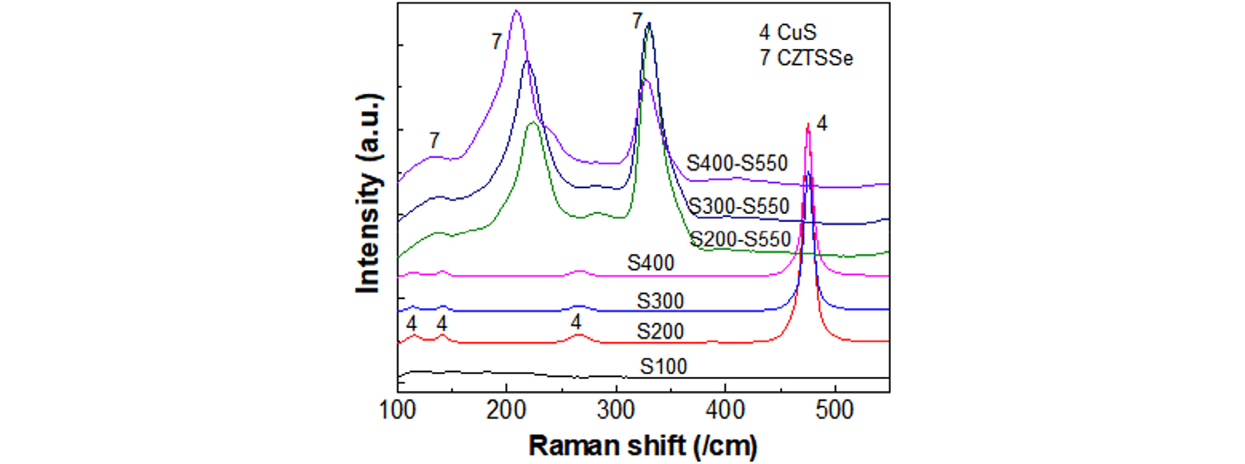
After the S-S annealing, only CZTSSe peaks were observed with the peaks around 135, 220 and 330 /cm. The shift of the Raman peaks in S200-S550, S300-S550, and S400-S550 films were small. Pure CZTSe has the main peak at 195 /cm and pure CZTS has the main peak 339 /cm26,27). Unlike pure CZTSe and CZTS, two strong peaks around 220 and 330 /cm were observed in the CZTSSe film with slight shift from pure CZTSe and pure CZTS. Since the intensity of these two peaks are similar, the overall S/(S+Se) ratio =0.47, in the CZTSSe zone in Fig. 6, seemed a reasonable value.
Fig. 9 shows the cross-sectional SEM images of the films after S pre-annealing at 200°C, 300°C and 400°C for 10 min (denoted as S200, S300, and S400, respectively). After 200°C pre-annealing, a CuS layer with a huge volume expansion was clearly observed due to sulfur incorporation into the thin Cu layer. No morphology change was observed in the SeSe2 layer and the demarcation between CuS and SnSe2 was clearly seen after 200°C pre-annealing. After 300°C pre-annealing, the thickness of CuS layer increased to larger than 1 μm, indicating that Cu was completely converted to CuS at 300°C. The demarcation between CuS and SnSe2 was partially destroyed in some region, indicating that a reaction between CuS and SnSe2 started.
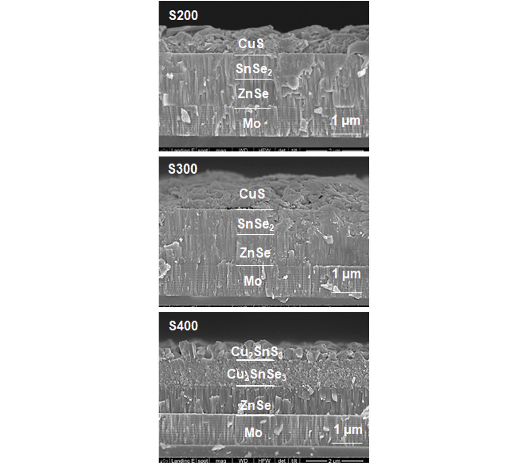
At 400°C, in the CuS layer (top layer), the small and agglomerated CuS grains changed to large columnar grains with big space between the grains, suggesting that SnSe2 diffused out from bottom layer to top layer to form a ternary phase Cu2Sn(S,Se)3. In the SnSe2 layer (bottom layer), the grains with as-sputtered SnSe2 columns changed to the grains with very small round shapes, suggesting that the CuS diffused into SnSe2 layer to form ternary phase Cu2Sn(S,Se)3. The thickness of the top layer decreased compared to that of CuS, probably due to densification, while that of bottom layer was unchanged. Note that the demarcation between SnSe2 and ZnSe was not changed, indicating that no reaction took place between SnSe2 and ZnSe up to 400°C.
Based on the analysis from the XRD patterns, Raman spectra, and SEM images, the reactions in the S-S annealing can be written as follows. At 200°C and 300°C, the Cu metal on the top of the Cu/SnSe2/ZnSe precursor was sulfurized first.
The thickness of the Cu layer increased from 0.2 μm to about 1 μm by the reaction (1). At 400°C, the CuS and SnSe2 reacted to form ternary phases.
At 550°C, the following reactions took place.
The observed S/(S+Se) values in the S-S annealing were ranged from 0.25 to 0.63 in Table 1. Especially, the value for S300-S550 was around 0.53, which was close to 0.5.
3.3 Phase evolution in the N-S annealing
Fig. 10 shows the XRD patterns of the as-deposited precursor film, S pre-annealed films, and N-S processed films. The samples N100, N200, N300, and N400 denoted for N pre-annealing at 200, 300, and 400°C for 10 min and the samples after S post-annealing at 550°C for 5 min (denoted as N200-S550, N300-S550, and N400-S550).
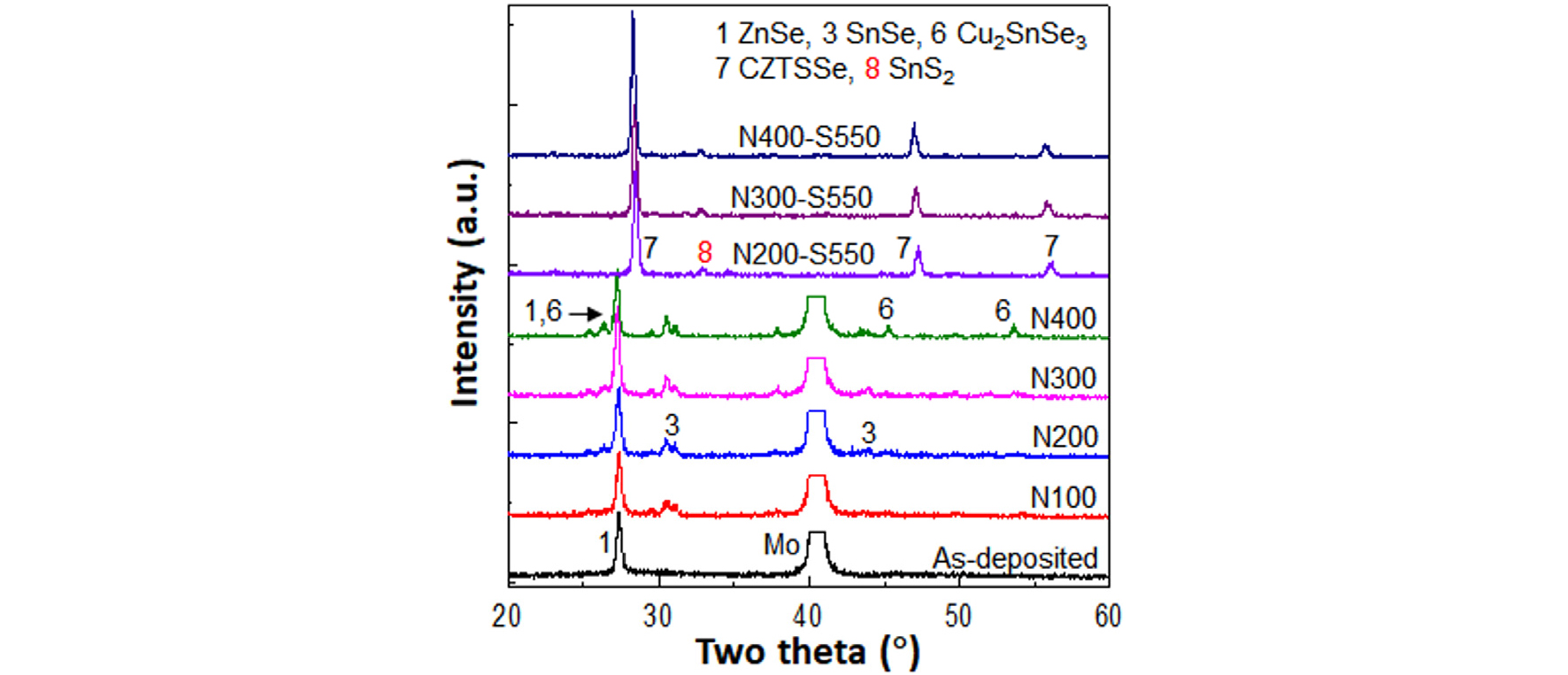
At 100, 200, and 300°C pre-annealing in N2, SnSe peaks were observed by partial crystallization in the amorphous SnSe2 layer. At 400°C, ternary CuSnSe3 phase was observed in addition to SnSe phase.
After 550°C annealing, two phases were observed: CZTSSe phase and SnS2 second phase. The SnSe phase formed during the N2 pre-annealing was the origin of the SnS2 generation. The plate-shaped SnS2 phase greatly degraded the not only surface morphology but also bulk morphology of CZTSSe film.
Fig. 11 shows the Raman spectra of the N2 pre-annealed films (N100, N200, N300, and N400) and N-S processed films (N200-S550, N300-S550, and S400-S550). At 200°C, the broad peaks around 120 /cm and 170 /cm correspond to SnSe2 phase in amorphous state. At 300°C, those peaks became sharper, implying the crystallinity of SnSe2 phase was improved by heating. At 400°C, the sharp peaks corresponding to Cu2SnSe3 and SnSe phases appeared.
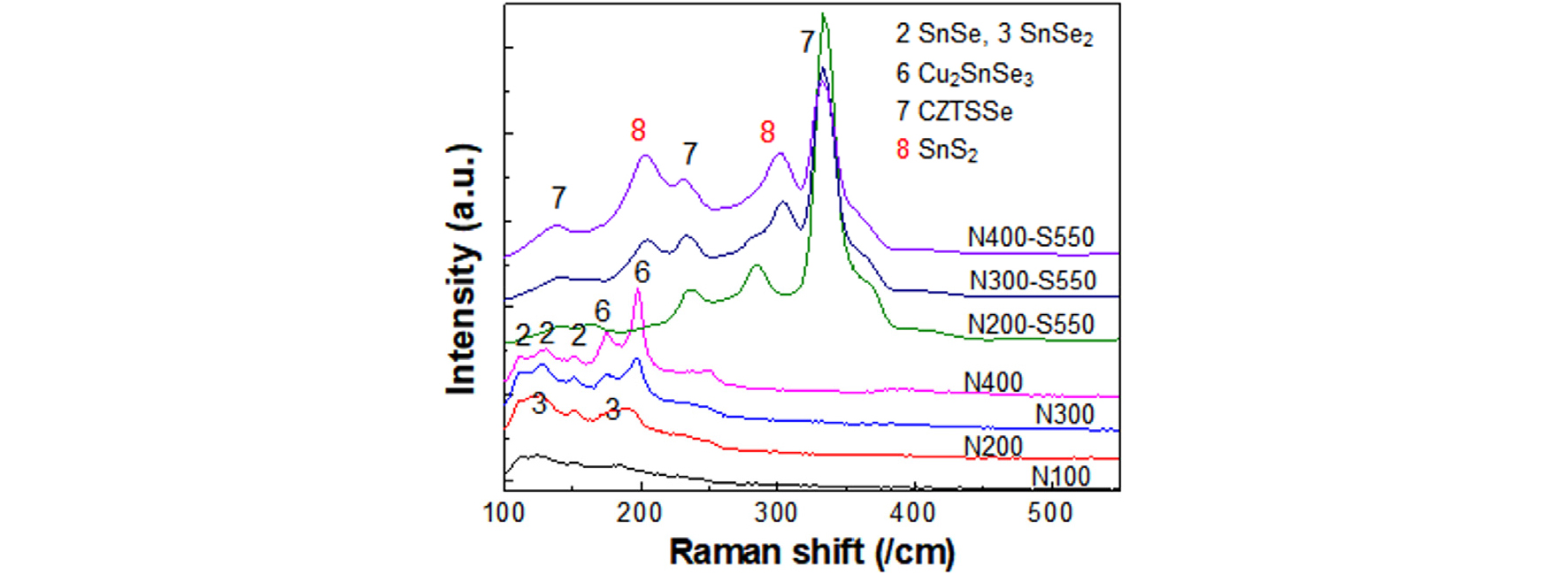
After N-S annealing (N200-S550, N300-S550, and S400-S550), four strong peaks were observed. The peaks at 220 and 330 /cm correspond to CZTSSe with S-Se solid solution28). And the peaks at 210 and 300 /cm correspond SnS2 second phase29). In the N-S annealing, ZnSe peak was not observed in Raman spectroscopy in Fig. 11, while a very strong peak near 27° was observed in the XRD patterns in Fig. 10. This indicates laser penetration was limited by surface Cu metal and ternary Cu2SnSe3 layer in the N2 pre-annealing.
Fig. 12 shows the cross-sectional SEM images of the films after N2 pre-annealing at 200°C, 300°C and 400°C for 10 min (denoted as N200, N300, and N400, respectively). At 200°C, the morphology of the amorphous SnSe2 layer changed from columnar to agglomerated grains, indicating that the stress generated during precursor deposition was released and a more stable SnSe phase was formed. At 300°C, the grains in the SnSe2 layer became bigger and more clearly demarcated among grains in the layer. But no morphological change was observed in the ZnSe layer up to 300°C.
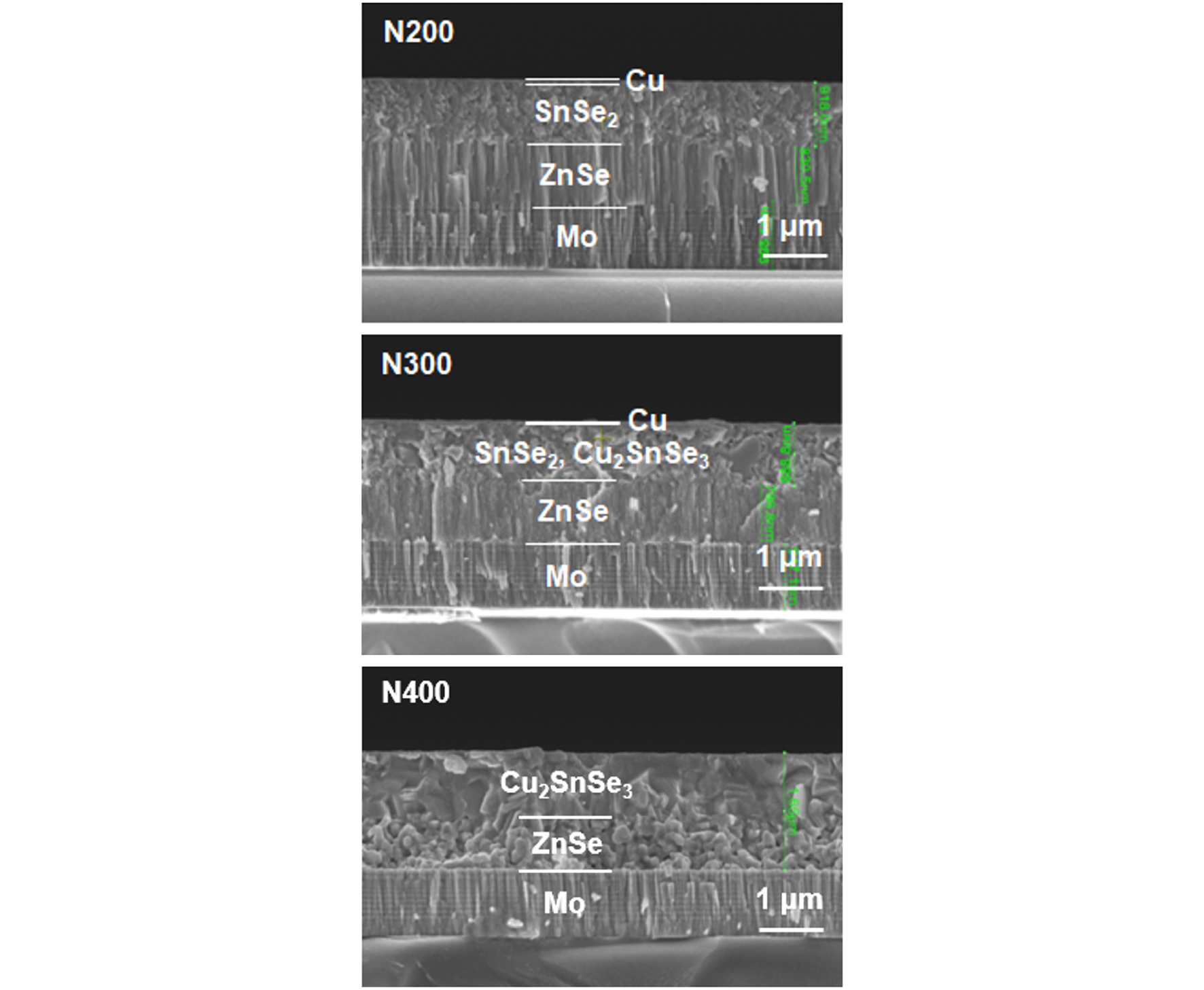
At 400°C, large grains were observed in the SnSe2 layer that converted to Cu2SnSe3 and SnSe phases, confirmed in XRD patterns in Fig. 8. It was also noted that the columnar morphology of ZnSe layer changes to small round-shaped grains. The morphology change in the ZnSe could be due to stress relaxation or Cu incorporation into ZnSe layer.
Based on the analysis from the XRD patterns, Raman spectra, and SEM images, the reactions in the N-S annealing can be written as follows. At 300°C and 400°C, Cu reacted with SnSe2 to form Cu2SnSe3 and SnSe second phase.
It was noted that the portion of the SnSe second phase was similar to that of Cu2SnSe3 phase.
At 550°C, all the selenide compounds were reacted with sulfur.
The S/(S+Se) values by the N-S annealing were 0.78 to 0.90 in Table 1. From eq. (5) and eq. (6), where 3 S and 1 Se from CZTSSe and 2 S from SnS2, the S/(S+Se) is 0.83. Especially, the value of 0.84 from N300-S550 sample was close to this value. It was seen that the morphology of CZTSSe film in the N-S annealing was aggravated by the formation of SnSe second phase during N2 pre-annealing and by the conversion to SnS2 second phase during S post-annealing.
3.4 Device performance
The CZTSSe film with the S-S annealing demonstrated a possibility of fabricating a densely-packed CZTSSe film with a smooth surface and large grains. On the other hand, the N-S annealing demonstrated a worst quality of CZTSSe film that consisted of plate-shaped grains on the surface and poorly connected debris grains in the bulk.
A CZTSSe solar cell using the CZTSSe film prepared by the S-S annealing was fabricated. Al-doped ZnO/i-ZnO/CdS layers were deposited on the CZTSSe/Mo/sodalime-glass substrate. A 70-nm thick CdS layer was deposited by chemical bath deposition. Then, 50-nm thick intrinsic ZnO and 200-nm thick Al-doped n-ZnO were deposited by RF sputtering. Then, Al as a top contact was deposited by electron beam evaporation using an aperture mask19). I-V measurements were performed on the solar cell under 1.5AM (1,000 W/m2) irradiation with a Mac Science solar simulator. The external quantum efficiency was measured with PV measurements using a spectral photocurrent meter.
Fig. 13 shows the current-voltage (I-V) curve (a) and external quantum efficiency (EQE) spectrum (b) of the CZTSSe solar cell using the CZTSSe film prepared by the S300-S550 annealing. From the I-V curve, the power conversion efficiency (PEC) was 1.9% for 0.44 cm2 with short-circuit current (Jsc) = 11.7 mA/cm2, open-circuit voltage (Voc) = 0.406 V, and fill factor (FF) = 0.42. The shunt resistance (Rsh) and series resistance (Rs) of the cell were 126.6 and 30.4 Ω·cm2, respectively. The Rsh value was too small and the Rs value was too large in the cell.
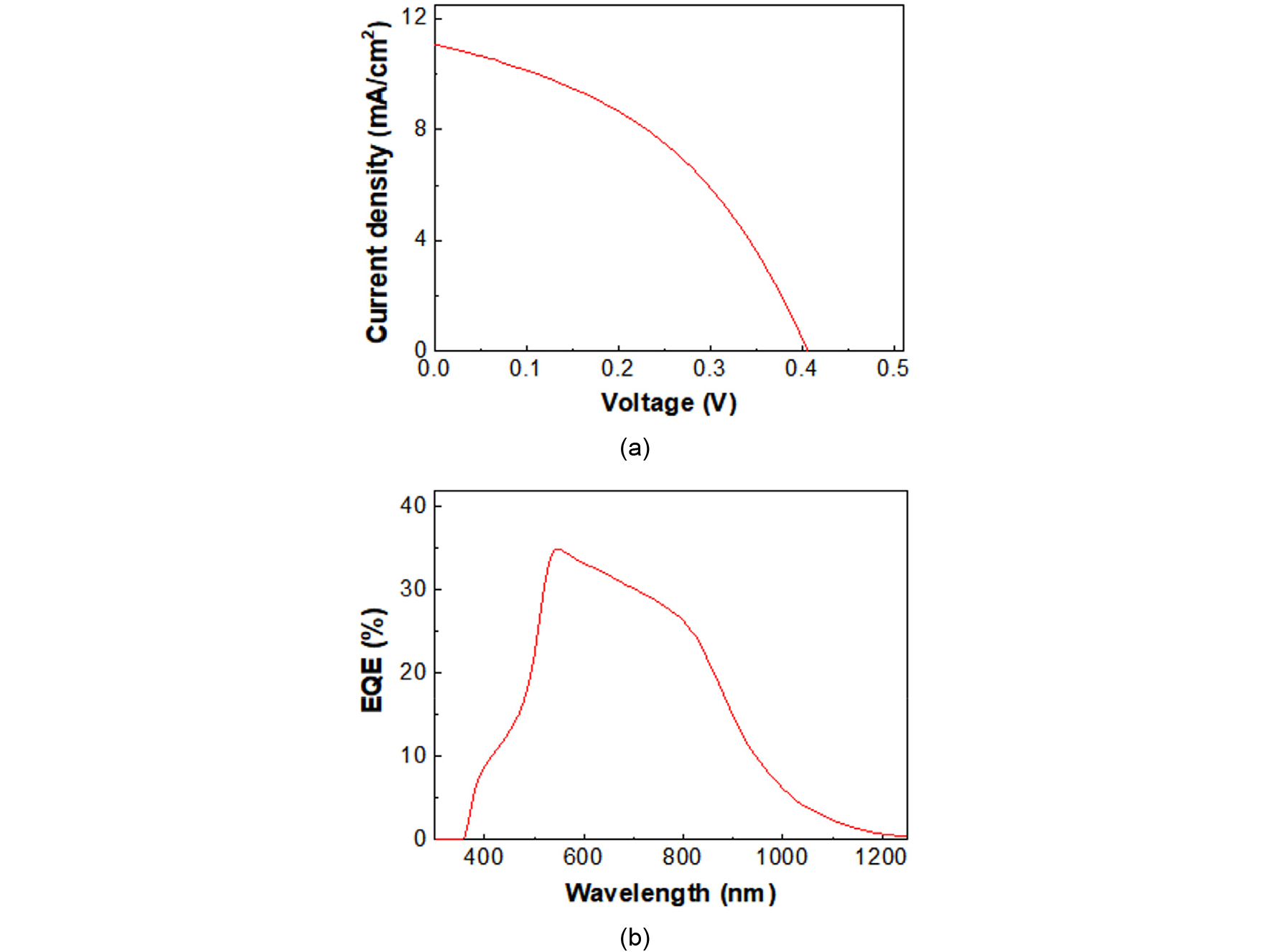
The EQE spectrum in Fig. 13(b) demonstrated that the overall value was low, suggesting that the Rs value should be further reduced. The extrapolation of the largest slope near 900 nm region suggested that the band gap of the CZTSSe was around 1.2 eV.
Even though the mixing of S and Se seemed work very well, the 1.9% PCE was much lower than our previous 4.7% PCE with metal precursor19). In our experiment, a remaining Zn(S,Se) that has a high resistivity could hurt current collection. Indeed, the Rs value of 30.4 Ω·cm2 was too large to get high performance. Controlling the thickness of Zn(S.Se) layer needs an elaborated and precise work. It is beyond the scope of this paper.
Even though this PCE value was much lower than current record efficiency of 12.6%, our two-stage S-S annealing by S pre-annealing and S post-annealing could be a useful stepstool for large-area production in the future.
From morphology point of view, in the S-S annealing, pinholes or volcano mouth were generated on the surface due to too much Se evolution. In that sense, replacing ZnSe by ZnS in the Cu/SnSe2/ZnSe precursor could be an interesting choice for further study and it is beyond the scope of this paper.
4. Conclusions
The morphologies of CZTSSe film prepared by S pre-annealing and S pre-annealing were very different. The S-S annealing (S pre-annealing and S post annealing) resulted in a dense CZTSSe film with a smooth surface. The N-S annealing (N2 pre-annealing and S pot-annealing) resulted in a porous CZTSSe film with a plate-like grains on the surface.
In the S-S annealing, CuS was formed first on the top of the precursor below 400°C and then reacted to form ternary Cu2Sn(S.Se)3 at 400°C. The ternary phase reacted with ZnSe to form CZTSSe at 550°C.
In the N-S annealing, Cu and SnSe2 reacted to form SnSe and Cu2SnSe3 at 400°C. At 550°C, the ternary phase reacted with ZnSe to form CZTSSe at 550°C, while SnSe converted to SnS2 that had a plate- shaped grains and severely aggravated the morphology of CZTSSe film.
The CZTSSe film prepared by the S-S annealing provided a good morphology. However, the PCE of the CZTSSe cell was 1.9%. One of the reasons of such low efficiency could be the existence of Zn(S,Se) layer between CZTSSe and Mo substrate. Our approach of using a Se-containing precursor for CZTSSe preparation demonstrated that the idea worked well regardless of low efficiency.
