

Nomenclature
Eg : band gap, eV
TRTA : RTA temperature, °C
VOC : open-circuit voltage, V
JSC : short-circuit current density, mA cm-2
Rs : series resistance, Ω·cm2
Rsh : shunt resistance, Ω·cm2
Subscript
SnS : Tin sulfide
CIGS : Cu(In,Ga)Se2
CdTe : Cadmium telluride
XRD : X-ray diffraction
FE-SEM : Field Emission Scanning Electron Microscopy
TCO : Transparent Conduction Oxide
FF : Fill Factor
PCE : Power conversion efficiency
RTA : Rapid thermal annealing
VTD : Vapor transport deposition
1. Introduction
In the last few decades solar electricity, as a good candidate of clean and renewable energy, have achieved significant progress1). In addition to conventional c-Si (single crystal silicon) solar cells, thin-film solar cells (TFSCs) have also been established in industry2-4). Recently, metal chalcogenide-based materials have emerged as a promising absorber for TFSCs due to toxic and rare earth elements present in established CdTe and CIGS TFSCs5-7). The optical energy band gap (Eg) of metal chalcogenide-based materials lies between 1.1 to 1.7 eV with a high absorption coefficient of ≥ 105 cm-1, making them favorable absorber candidates for next generation TFSCs8-9). Among these metal-chalcogenide-based materials, tin sulfide (SnS) has emerged as promising absorber material for TFSCs owing to its excellent optical and electrical properties and intrinsically having p-type carrier concentration with excellent stability10-11). SnS has scalable potential to fulfill material demand for the thin-film device industry as it contains non-toxic and earth abundant elements12-13). The electronic properties of absorber material influence the performance of TFSCs largely. The SnS thin film deposited on Mo by vapor transport deposited (VTD) has a bandgap of about 1.3 eV and solar radiation absorption power of about (≥ 105 cm-1) which is most favorable for TFSCs14). However, except few cases in which power conversion efficiency (PCE) is above 4.0%, the performance of SnS based solar cells are mostly below 4.0%. More recently, Yun et al. reported a record PCE of 4.8% for SnS/TiO2 based heterojunction15). Moreover, the PCE of these high performance SnS TFSCs remains far below the theoretical reported value of ~32.0%. Such lower performance of SnS-based TFSCs is mainly due to lower short-circuit current density (JSC) value, lower minority carrier lifetime, owing to higher recombination rate assisted by multi-defect states present in absorber and unfavorable conduction band offset (CBO) with n-type buffer16-17).
SnS thin films can be deposited using various deposition processes, including chemical deposition as well as physical vacuum-based deposition process18-20). Low complexity, conformal growth, low cost, and ease in handling stoichiometry of film, vacuum deposition processes have great importance21). As a versatile and cost effective method to deposit thin films, VTD has attracted much attention among other vacuum techniques14). VTD deployed commercially available high purity material as a target; thus, conformal surface properties with high purity and compact thin film were deposited with high speed of deposition18). VTD is also for commercial application in the thin-film industry17,22).
SnS deposited by VTD demonstrate a dense and flat surface film with minimum pinholes, which help in the improvement of cell performance18). Although from VTD a compact, dense surface morphology film was obtained, but the JSC of the device remains low enough in comparison to other materials with the same range of energy bandgap21).
Here, we demonstrate a path to enhance JSC of VTD grown SnS-based TFSCs by Se incorporation in SnS absorber. Se incorporation in the SnS thin film was carried out in two steps. First SnS was deposited on Mo coated glass substrates (Mo/SLG) and after that rapid thermal annealing (RTA) was deployed to defuse Se powder in the SnS absorber. It was observed that the TRTA strongly influence the performance of device, specially JSC enhanced in sufficient amount.
2. Experimental procedure
A one zone VTD furnace was deployed to deposit SnS absorber on aMo/SLG. Before SnS deposition, Mo/SLG substrate was sequentially cleaned by isopropyl alcohol (IPA) and deionized (DI) water for 15 min each in an ultrasonication bath and dried in nitrogen gas flow. A ceramic boat containing 0.3 g of SnS powder (5N) was loaded in the middle of heating zone of the VTD furnace.
Furthermore, clean Mo/SLG was substrate put on a quartz substrate holder placed at the one end of heating zone of the VTD furnace and maintained the approximate distance of 10 cm between source and substrate. Then, a mechanical pump was used to evacuate the chamber up to a base pressure of 5.0 mTorr. Next, a flow of Ar gas was introduced in the chamber and a 2.0 Torr controlled and stabilized pressure flow was maintained inside the chamber. After that the furnace was allowed to heat up to 600°C at a ramping rate of 30°C per min and maintained at 600°C for 30 min. After the completion of deposition process furnace was allowed to cool down to room temperature, and samples were removed, and seal packed up to further device fabrication process. The Se incorporation in the film was carried out using tube furnace RTA at different temperatures. A graphite box contains 0.1 g of Se powder uniformly around the corner and sample was placed at the center of box and placed at the center of RTA furnace. The annealing temperature varied from 300°C to 400°C and annealing time of 300 s and ramping time of 20 s in an Ar flow of 50 sccm remains fixed for all the sample. A schematic of Se-incorporation by RTA is shown in Fig. 1a.
The chemical bath deposited (CBD) CdS layer was deployed to form heterojunction with SnS deposited on Mo/SLG substrate. The proximate thickness of the CdS layer was about 50 nm23). Finally, radio frequency sputter was used to deposit transparent conducting oxide (TCO) film with combination of intrinsic zinc oxide (i-ZnO) of about 45 nm and Al-doped zinc oxide (AZO) of about 350 nm thickness23). Al finger electrode were deposited as front contact using DC sputter to fabricate a solar cell in the configuration of (Al/AZO/i-ZnO/CdS/Se-graded SnS/Mo/SLG). The schematic device structure is shown in Fig. 1b.

Approximate thickness and surface morphology of Se-incorporation inside SnS layer was studied using field emission scanning electron microscope (FE-SEM, ZEISS Gemini 500). Crystal structure and peak pattern of Se-graded SnS film deposited on different substrate was carried out using X-ray diffraction and grazing incidence angle GIXRD (XRD; PANalytical PANalytical X'Pert PRO MPD) with Cu-Kα radiation of 1.5406 Å. A solar simulator (San-ei Electric XES-301S, 100 mW cm-2) and Keithley 2400 source meter were utilized to measure the current density-voltage (J-V) characteristic under one sun illumination. The external quantum efficiency (EQE) of devices was carried out using IPCE solar simulator (MacScience, K3100 EQX, IPCE Solar Simulator).
3. Result and discussion
The FE-SEM micrograph of top view microstructure of pristine and Se graded SnS film prepared at different TRTA were analyzed as shown in Fig. 2(a-d) for 300°C, 350°C, and 400°C respectively. It was observed that at TRTA of 300°C, the grain size of film was lower compared to pristine film, while beyond the TRTA of 300°C grain size gradually increases. This may be due to the adsorption of Se atoms in the voids present in the film. Also, the surface of the film may be covered with secondary phase crystallites24-25).
Also, the structure of the film changes from cube-like to plate like with an increase in TRTA, as evident in SEM top surface morphology. In addition, cross-section of pristine as well as Se-graded SnS on Mo/SLG substrate for TRTA 300°C, 350°C, and 400°C were studied as shown in Fig. 2(e-h) using FE-SEM. The elemental mapping of the prepared Se incorporated SnS thin films was performed using Energy Dispersive X-Ray Spectroscopy (EDS) to confirm chemical composition, as shown in Fig. 2(i-l). With an increase in the TRTA, the Se incorporation was found to be increased within the SnS with a decrease in the S content. From the EDS analysis, the Se/(Se+S) ratio was obtained to be 0.57, 0.74, and 0.86 for TRTA of 300°C, 350°C, and 400°C, respectively. The diffusion of Se inside the film was strongly influenced by TRTA, which is also evident in cross-sectional FE-SEM image. It was identified that the density of the film increases owing to reduction in voids with increase in TRTA26).
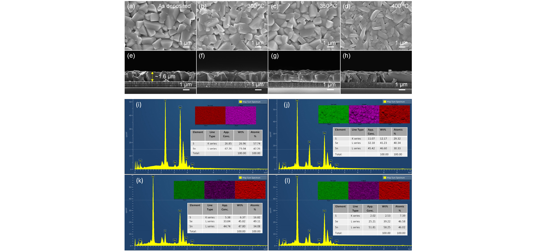
Fig. 2
FE-SEM image of Se graded SnS top surface morphology (a) As deposited VTD-SnS, (b) 300°C TRTA, and (c) 350°C TRTA, and (d) 400°C TRTA, and cross-section view (e) As deposited VTD-SnS, (f) 300°C TRTA, (g) 350°C TRTA, and (h) 400°C TRTA and EDS elemental mapping of (i) As deposited SnS, and selenized SnS at (j) 300°C TRTA, (k) 350°C TRTA, and (l) 400°C TRTA
The structural characterization of the pristine and Se-graded SnS film was carried out using X-ray diffraction and grazing incidence angle (GI-XRD) with an incident angle of 0.5° for the film prepared at different TRTA as shown in Fig. 3(a, b). Diffraction patterns indicate SnS thin film (JCPDS; 00-039-0354) with slightly shifted peak position, and as the TRTA increases a distorted peak of SnSe (JCPDS; 00-048-1225) was observed in XRD patterns which confirms the diffusion of Se in SnS thin film. Some weak XRD peaks of SnSe2 were also observed. All the diffraction patterns confirm diffusion of Se inside the film. GI-XRD of as deposited VTD-SnS as well as Se incorporated samples at different TRTA was carried out. As clear from Fig. 3(b) with TRTA the distortion in peak position is observed. The secondary phases get intensify with TRTA.
The rough estimation of the particle size was calculated from crystallite size obtained from XRD analysis. The crystallite sizes were calculated using the Scherrer formula27).
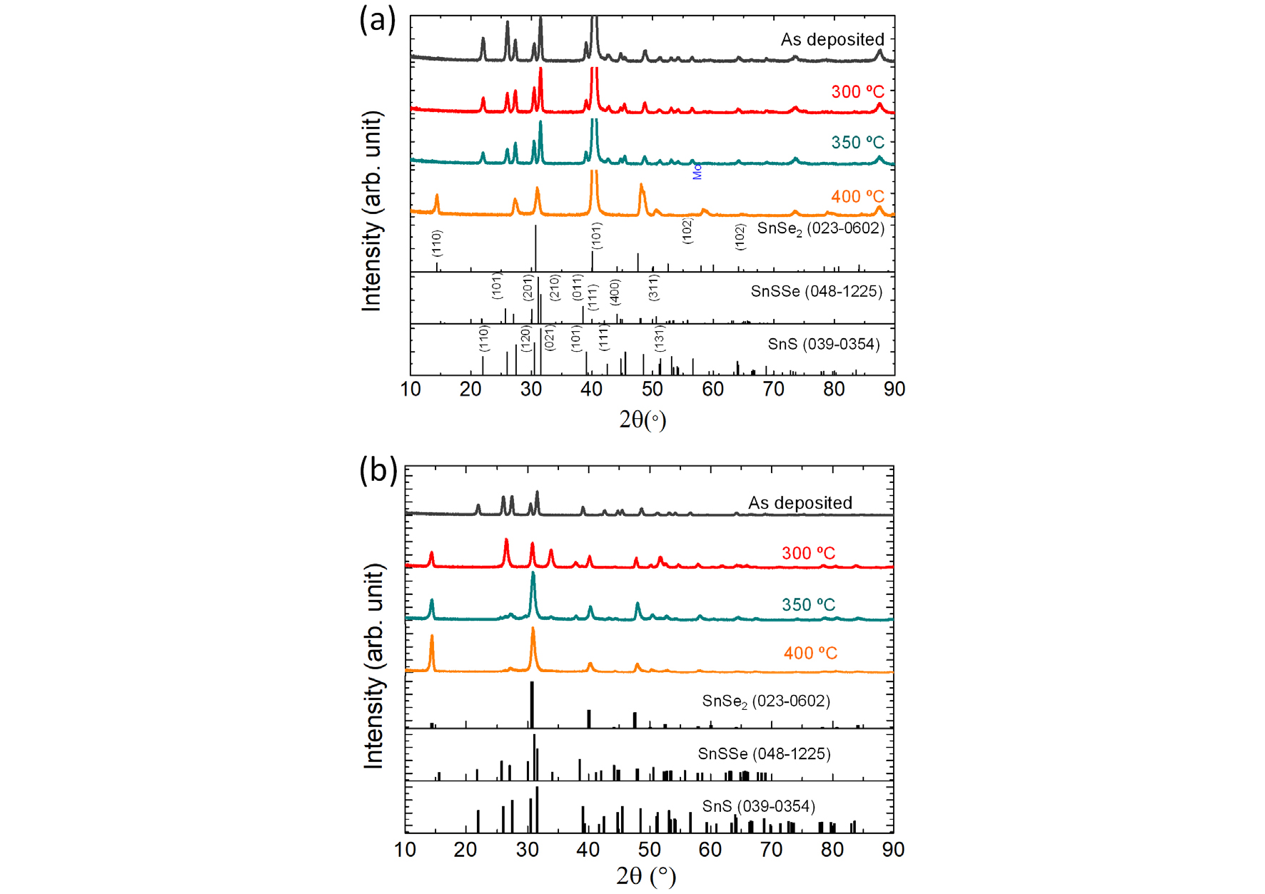
where K is particle shape factor, λ is X-ray wavelength, βhkl is full width at half maxima of obtained XRD peak, and θ is Bragg's diffraction angle. The calculated crystallite size of SnSSe films decreased from 19.6 nm for 300°C TRTA to 17.6 nm for 400°C TRTA. During selenization, the Se molecules were diffused owing to thermal kinetics and rearranged to form larger-sized crystal grains. Further increasing the selenization temperature from 300°C to 400°C, leads to a more dense and uniform crystalline thin film from cube-like to ellipsoid growth of grains with an increase in grain size, which is advantageous for suppressing the recombination loss at the grain boundaries. In the selenization process, recrystallization of film leads to formation of secondary phases as evident in GI-XRD pattern28).
The photovoltaic characteristic of the prepared device with Se incorporated SnS absorber at TRTA from 300 to 400°C and pristine samples were measured by utilizing our installed solar simulator as shown in Fig. 4(a-d) respectively. As TRTA increases, the JSC of the device increases leading to an increase in the performance of the solar cell. Also, with increase in TRTA, VOC and FF of the device decreases Fig. 4(a-b). Generally, it was observed that Se incorporation inside chalcogenide absorber material led to increase in JSC while a loss in VOC also observed at the same time29-30). The anticipated trend of decreasing VOC and increasing JSC with Se incorporation is observed. The Se incorporated device has a higher JSC compared to the pristine SnS devices, which is explained by an improved collection at the long wavelengths31). The improved collection could be associated with the back surface field provided by Se incorporation, as with increase in TRTA diffusion of Se also increases as observed in EDS analysis. A similar trend was observed in some previous reports32-35). The PV parameters for champion cells are listed in Table 1. The PV properties of the device were studied by light J-V characteristic of pristine VTD-SnS and Se incorporated VTD-SnS at TRTA as an absorber material, as shown in Fig. 5(a). With an increase in TRTA from 300°C to 400°C, decreasing trend in VOC from 0.290 V to 0.140 V was observed, as seen in Fig. 5(a). The device with Se incorporation at 300°C TRTA shows a slightly increased VOC than the pristine SnS device. The Dark J-V characteristic was carried out to recognize this behavior. The interface quality of the junction improves with the incorporation of Se in the VTD-SnS at 300°C TRTA, in comparison to other devices which was observed in the dark J-V characteristic Fig. 5(b). An increase in JSC with the increase in TRTA takes place from 18.6 to 23.0 mA cm-2, which would be attributed to an increase in photo-generated current with an increase in Se content inside the film34,36. To understand the photogenerated current and charge collection behavior of devices EQE measurement from a wavelength of 300 nm to 1400 nm was carried out Fig. 5(c). The device with Se incorporation shows better charge collection17,35). A highest JSC of 23.1 mA cm-2 with a VOC of 0.140 V, FF of 43.3% and PCE of 1.38% for the TRTA of 400°C, while highest performance of 2.21% with JSC of 18.6 mA cm-2, VOC of 0.290 V, and FF of 40.9% was observed at a TRTA of 300°C. EQE had deployed to calculate the bandgap of pristine and Se incorporated samples at different TRTA shown in Fig. 5(d). The approximate bandgap of prepared SnS is 1.323 eV, 300°C TRTA is 1.316 eV, 350°C TRTA is 1.279 eV, and 400°C TRTA is 1.273 eV.
Table 1.
Photovoltaic parameters for Se graded SnS absorber via RTA at different TRTA
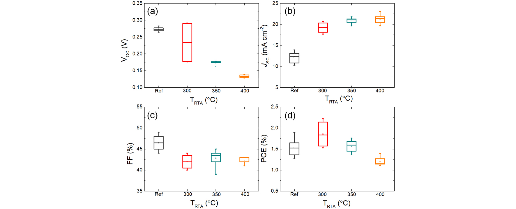
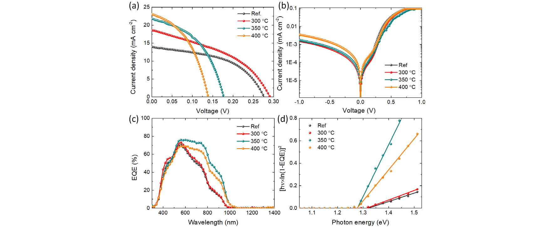
The increment in the JSC would be attributed to the reduction in the band gap of materials, which led to increment in absorption of solar radiation with the incorporation of Se inside the SnS thin film, which may extend the absorption range to higher wavelength. The loss in VOC and FF may also attribute to reduction in bandgap as well as shunt resistance of the device.
4. Conclusion
In conclusion, the JSC of SnS-based thin film solar cells was improved significantly by Se incorporation in SnS thin films using RTA. The diffusion of Se from the top of SnS thin film through selenization using RTA was evident in the XRD of the film. The diffusion of Se strongly depends on TRTA. As TRTA increases, the diffusion of Se also increases. It is observed that film structure changes from cube-like to plate-like structure with TRTA. The Se-graded SnS absorber film was used for device fabrication, which is favorable for band alignment as well as optical response. Consequently, Se-graded SnS absorber shows high JSC, which leads to comparatively better performance of device. The increase in JSC was compensated with loss in VOC of the device. The maximum JSC of 23.1 mA cm-2 was observed for 400°C at the same time VOC reduces to 0.140 V. The highest performance of 2.21% with JSC of 18.6 mA cm-2, VOC of 0.290 V and FF of 40.9% is observed for an RTA temperature of 300°C.
