

1. Introduction
2. Experimental
2.1 Device fabrication
2.2 Device characterization
3. Results and Discussion
4. Conclusion
1. Introduction
Enhancing the power conversion efficiencies (PCEs) and reducing the production costs of solar cells are crucial to secure market competitiveness in the solar cell market, which requires saving materials, reducing process times, lowering manufacturing costs, and reducing energy payback times. Kesterite thin-film solar cells based on Cu2ZnSnS4 (CZTS) and related materials (e.g., CZTS, Cu2ZnSnSe4 (CZTSe), and Cu2ZnSn(S,Se)4 (CZTSSe)) are advantageous because they are cheaper than conventional thin-film solar cells based on CdTe or Cu(In,Ga)Se2 (CIGS)1). As shown in Table 1, CZTS-based thin-film solar cells with an absorber layer thickness of 2 μm or higher have PCEs of 10% or higher2-6). Liu et al. reported an 8.57% PCE for a CZTS thin-film solar cell with an absorber thickness of 0.8 μm by introducing an Al2O3 intermediate layer between Mo and CZTS7). Shin et al. fabricated CZTS thin-film solar cells with thin absorber (~ 0.6 μm) layers and PCEs of up to 8.4% using a vacuum thermal evaporation method8). Yang et al. reported a 7.5% PCE for a CZTS thin-film solar cell with an absorber thickness of 0.58 μm by varying the sulfurization temperature9). CZTS thin-film solar cells with PCEs of 5.2%10) and 1.85%11) have been reported for absorber thicknesses less than 0.5 μm. PCEs of 22.6% have been reported for absorber layer thicknesses in the range of 2.5 to 3.0 μm12) for CIGS thin-film solar cells. However, the PCE decreases to 17.5% with an absorber layer thickness of 0.93 μm13) and to 13.5% for an absorber layer thickness of 0.385 μm14). Previous studies identified the following reasons for the decrease in the PCE with decreasing absorber layer thickness in CIGS thin-film solar cells: influence of the back contact15-20), absorber layer18, 20-25), buffer layer26-28), and transparent conducting layer18). However, no studies have investigated the change in the characteristics of CZTSe-based thin-film solar cells with decreasing absorber layer thickness. In this study, we investigated the CZTSe thin-film solar cells with an absorber layer thickness in the submicron range by examining the characteristics of the devices according to changes in the CZTSe absorber layer thickness.
Table 1.
Device characteristics of CZTS-based thin-film solar cells with various absorber layer thicknesses
2. Experimental
2.1 Device fabrication
Five samples were fabricated to compare the characteristics of CZTSe thin-film solar cells that have various absorber thicknesses. The structures of the solar cell devices comprised a soda lime glass (SLG) substrate, a 500-nm-thick Mo layer as the back-contact, an absorber layer, a 50-nm-thick CdS buffer layer deposited via a chemical bath method, a 50-nm-thick intrinsic ZnO layer deposited via sputtering, a 300-nm-thick Al-doped ZnO (AZO) transparent conducting oxide layer deposited via sputtering, and a 500-nm-thick Al collection grid deposited via thermal evaporation. The Mo layer was deposited on the SLG substrate via direct current magnetron sputtering using a Mo target of 99.99% purity. Metal precursors were deposited on the Mo layer using 99.99% pure Cu, Zn, and Sn sputtering targets with different thicknesses. The layers were deposited under sputtering powers of 150, 300, and 300 W for the Cu, Zn, and Sn targets, respectively, at a working pressure of 1 mTorr in an Ar atmosphere. The following precursor stacking orders were employed: SLG/Mo/Zn (198 nm)/Sn (281 nm)/Cu (168 nm), labeled CZTSe1; SLG/Mo/Zn (99 nm)/Sn (141 nm)/Cu (84 nm), labeled CZTSe2; SLG/Mo/Zn (49 nm)/Sn (71 nm)/Cu (42 nm), labeled CZTSe3; SLG/Mo/Zn (26 nm)/Sn (36 nm)/Cu (21 nm), labeled CZTSe4; and SLG/Mo/Zn (10 nm)/Sn (14 nm)/Cu (8 nm), labeled CZTSe5. These precursor films were selenized at atmospheric pressure using Se pellets (0.65 g) in an Ar-filled rapid thermal processing (RTP) chamber at a temperature of 510°C. The samples were heated from room temperature to 370°C for 1000 s and then maintained at 370°C for 1500 s. Subsequently, the samples were heated from 370°C to 510°C for 1000 s and then maintained at 510°C for 1100 s. A 50-nm-thick CdS buffer layer was deposited using chemical bath deposition from a bath containing cadmium sulfate (CdSO4), ammonium hydroxide (NH4OH), thiourea (NH2CSNH2), and DI H2O. The bath solution was composed of 732 mL of DI H2O, 80 mL of NH4OH, 100 mL of CdSO4 (0.015 M CdSO4), and 50 mL of NH2CSNH2 (1.5 M NH2CSNH2). The solution was heated in a bath and continuously stirred till the required deposition temperature was reached, and the temperature was controlled to within ± 1°C at 65°C. Subsequently, a 50-nm-thick intrinsic ZnO layer and a 300-nm-thick AZO layer were deposited via radio frequency sputtering. The AZO layer was deposited under a sputtering power of 200 W at a working pressure of 2 mTorr at a temperature of 200°C for 3000 s. Finally, a 500-nm-thick Al collection grid was deposited on top of the device using thermal evaporation.
2.2 Device characterization
The samples were characterized using scanning electron microscopy (SEM), a solar simulator, external quantum efficiency (EQE) measurements, and scanning transmission electron microscopy-energy dispersive spectrometry (STEM-EDS). Cross-sectional and surface images of the absorber layers were obtained using SEM (S-4800, Hitachi Co., Japan). The current-voltage (I-V) characteristics were determined under a simulated air mass 1.5 global spectrum (AM 1.5 G) and an illumination of 100 mW/cm2 (1 sun) at a temperature of 25°C using a solar simulator (94022A, Newport Co., USA). The EQE values were obtained using a lock-in amplifier system (SR 830 DSP, McScience Inc., South Korea) operated at a sensitivity of 100 mV/nA. STEM-EDS measurements were performed using a QUANTAX 200 system (Bruker Co., USA) to analyze the compositions of the absorber layers and map the elemental distributions.
3. Results and Discussion
Fig. 1 shows SEM images of absorbers with various CZTSe absorber layer thicknesses. After selenization, the thicknesses of the CZTSe absorber layers are as follows: CZTSe1, 2.78 μm (Fig. 1 (a)); CZTSe2, 1.01 μm (Fig. 1 (b)); CZTSe3, 0.55 μm (Fig. 1 (c)); CZTSe4, 0.29 μm (Fig. 1 (d)); and CZTSe5, 0.15-0.23 μm (Fig. 1 (e)). Fig. 1 (f) shows that as the CZTSe absorber layer thickness decreases, the grain sizes and crystal orientation peak intensities of CZTSe (101), CZTSe (112), CZTSe (204), and CZTSe (312) decrease. This indicates that the absorber layer’s crystal growth is affected by the its thickness.
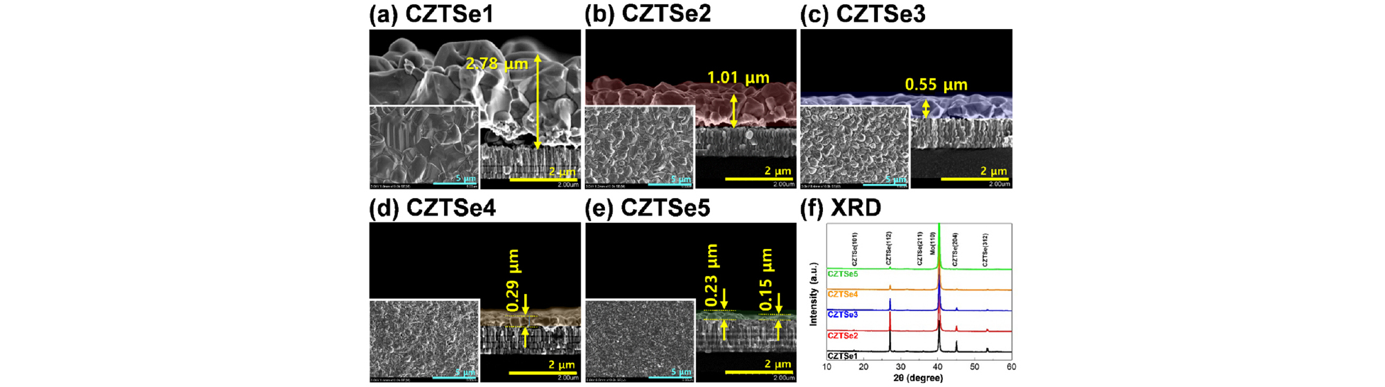
Fig. 2 and Table 2 show the properties of the photovoltaic devices with various CZTSe absorber layer thicknesses. Figs. 2 (a), (b), and (c) show the I-V, EQE, and bandgap (Eg) characteristics with the highest PCEs, respectively. Fig. 2 (a) shows that the PCEs decrease from 10.45% (CZTSe1) to 1.54% (CZTSe5) as the CZTSe absorber layer thickness decreases, and Fig. 2 (b) shows that the EQEs decrease in all wavelength ranges. In addition, as shown in Fig. 2 (c), Eg increases from 1.069 eV (CZTSe1) to 1.096 eV (CZTSe5). Figs. 2 (d) - (h) show the statistical device characteristics for 16 devices of each absorber thickness. As the thicknesses of the CZTSe absorber layers decrease, the efficiency (Fig. 2 (d)), open-circuit voltage (VOC) (Fig. 2 (e)), current density (JSC) (Fig. 2 (f)), fill factor (FF) (Fig. 2 (g)), and VOC deficit (Eg/q - VOC) characteristics decrease. In particular, the decreases observed in the VOC, JSC, and VOC deficit are significant. As shown in Fig. 1 (f), the grain size decreases as the CZTSe absorber layer thickness decreases. This can lower the density of the absorber layer and cause a decrease in light absorption. In addition, an increase in grain boundaries due to a decrease in the grain size may cause current loss due to electron-hole recombination29). In particular, a large EQE loss is observed in the long-wavelength region (≥ 800 nm), as shown in Fig. 2 (b), for CZTSe4 and CZTSe5 with absorber thicknesses less than 0.29 μm. This tendency is observed because the electron-hole generation near the back contact increases as the absorber thickness decreases, and the current loss increases owing to the increase in back contact recombination20, 22). In addition, an increase in the reflection at the back contact electrode according to a decrease in the absorber thickness can cause a current loss in the long-wavelength region30).
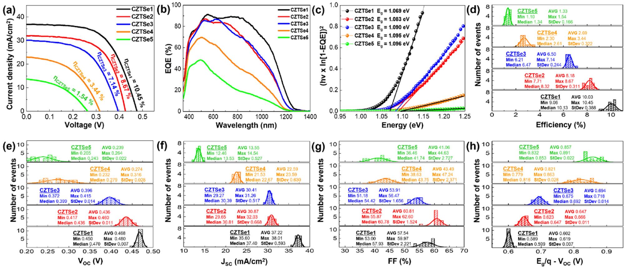
Fig. 2
Photovoltaic properties of devices with various CZTSe absorber layer thicknesses. (a) Current density-voltage curves, (b) EQE curves at a bias of 0 V, and (c) calculated bandgaps with the highest efficiencies. Statistical average values of the (d) efficiency, (e) VOC, (f) JSC, (g) FF, and (h) VOC deficit (Eg/q - VOC) for 16 devices of each thickness
Table 2.
Characteristics of devices with various CZTSe absorber layer thicknesses. All samples have a cell area of 0.185 cm2
The formation of secondary phases in the CZTSe absorber layer can interfere with the carrier flow, causing current loss31) and the formation of defects and defect clusters that can deteriorate the VOC and VOC deficit characteristics9, 31-34). We performed STEM-EDS mapping (Fig. 3-Fig. 7) to investigate the phase characteristics of the CZTSe absorber.
As shown in Fig. 3 (a), voids are observed in CZTSe1 at the absorber layer-back contact interface. Cu in the precursor reacts with Zn and Sn to form Cu5Zn8 and Cu6Sn5 alloy and forms Cu2Se during the selenization process. During this process, the Cu5Zn8, Cu6Sn5 alloy, and Cu2Se react with Se, generating VCu (Cu vacancies)35, 36). As VCu diffuses below the absorber layer via the Kirkendall effect, voids are formed at the absorber layer-back contact interface35, 37, 38). Figs. 3 (b) - (g) show that secondary phases are observed at the absorber layer-back contact interface. Fig. 3 (h) shows the formation of a 0.9 μm-thick MoSe2 layer. This is the result of a reaction between CZTSe and the Mo back contact and the decomposition and growth of CZTSe and MoSe2 during the selenization process39, 40). In Fig. 3 (i), in the lateral direction c→d, no secondary phase is observed, and the average atomic percentages of Cu, Zn, Sn, and Se are 26.3%, 14.5%, 11.0%, and 48.2%, respectively. Fig. 3 (j) shows that the average compositional ratios of [Cu]/([Zn]+[Sn]), [Zn]/[Sn], and ([Cu]+[Zn]+[Sn])/[Se] are 1.03, 1.32, and 1.07, respectively, and [Zn]/[Sn] has minimum and maximum values of 0.93 and 1.79, respectively, with a median of 1.35 and an average of 1.32. As shown in Fig. 3 (h), in the vertical direction e→f where no secondary phase is observed, the average atomic percentages of Cu, Zn, Sn, and Se are 25.7%, 14.2%, 11.8%, and 48.3%, respectively. Finally, Fig. 3 (k) shows that the average compositional ratios of [Cu]/([Zn]+[Sn]), [Zn]/[Sn], and ([Cu]+[Zn]+[Sn])/[Se] are 0.99, 1.20, and 1.07, respectively. Therefore, similar average compositional ratio characteristics are observed in the lateral and vertical directions with no secondary phase.
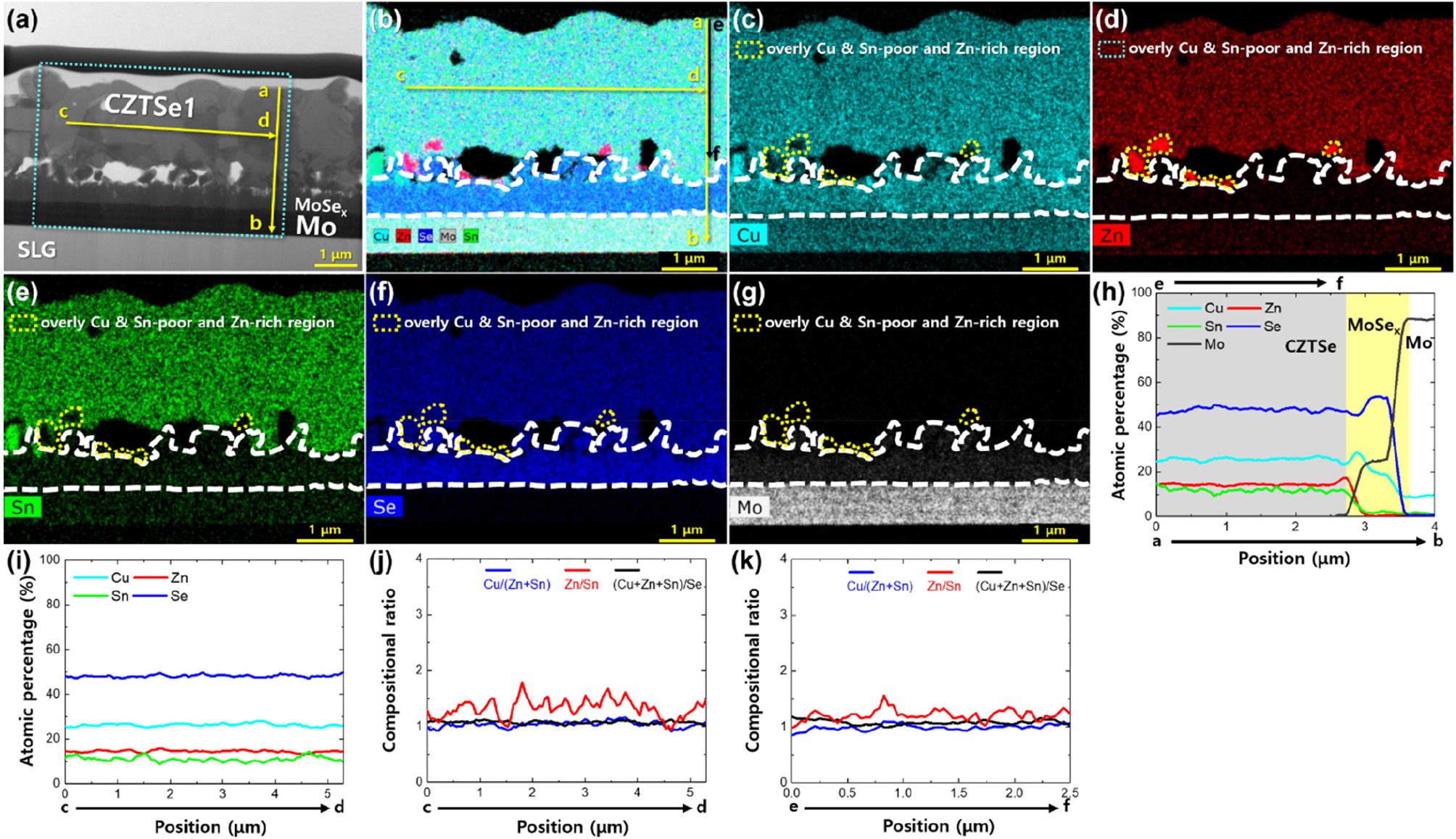
Fig. 3
STEM-EDS mapping images of CZTSe1 thin-film solar cells. (a) Cross-sectional STEM image. EDS mapping images of the CZTSe1 absorber layer showing mappings of (b) Cu, Zn, Sn, Se, and Mo, (c) Cu, (d) Zn, (e) Sn, (f) Se, and (g) Mo. The elemental variations in the vertical and lateral directions in (a) and (b) were measured using EDS line scans. EDS line scans along (h) a→b and (i) c→d. Compositional ratio variations along (j) c→d and (k) e→f
Similar to CZTSe1, voids (Fig. 4 (a)) and secondary phases (Figs. 4 (b)-(g)) are observed at the absorber layer-back contact interface of CZTSe2. Fig. 4 (h) shows the formation of a 0.4 μm-thick MoSe2 layer. As shown in Fig. 4 (i), in the lateral direction c→d where no secondary phase is observed, the average atomic percentages of Cu, Zn, Sn, and Se are 26.9%, 14.1%, 11.3%, and 47.7%, respectively. Fig. 4 (j) shows that the average compositional ratios of [Cu]/([Zn]+[Sn]), [Zn]/[Sn], and ([Cu]+[Zn]+[Sn])/[Se] are 1.06, 1.25, and 1.10, respectively, with [Zn]/[Sn] displaying minimum and maximum values of 0.99 and 1.86, respectively, along with a median of 1.24 and an average of 1.25 in the average compositional ratio distribution. As shown in Fig. 4 (h), in the vertical direction e→f where no secondary phase is observed, the average atomic percentages of Cu, Zn, Sn, and Se are shown to be 27.0%, 13.9%, 11.4%, and 47.7%, respectively. As shown in Fig. 4 (k), the average compositional ratios of [Cu]/([Zn]+[Sn]), [Zn]/[Sn], and ([Cu]+[Zn]+[Sn])/[Se] are 1.07, 1.22, and 1.10, respectively. Therefore, it can be concluded that the average compositional ratio characteristics are relatively similar in the lateral direction c→d and vertical direction e→f where no secondary phase is observed.
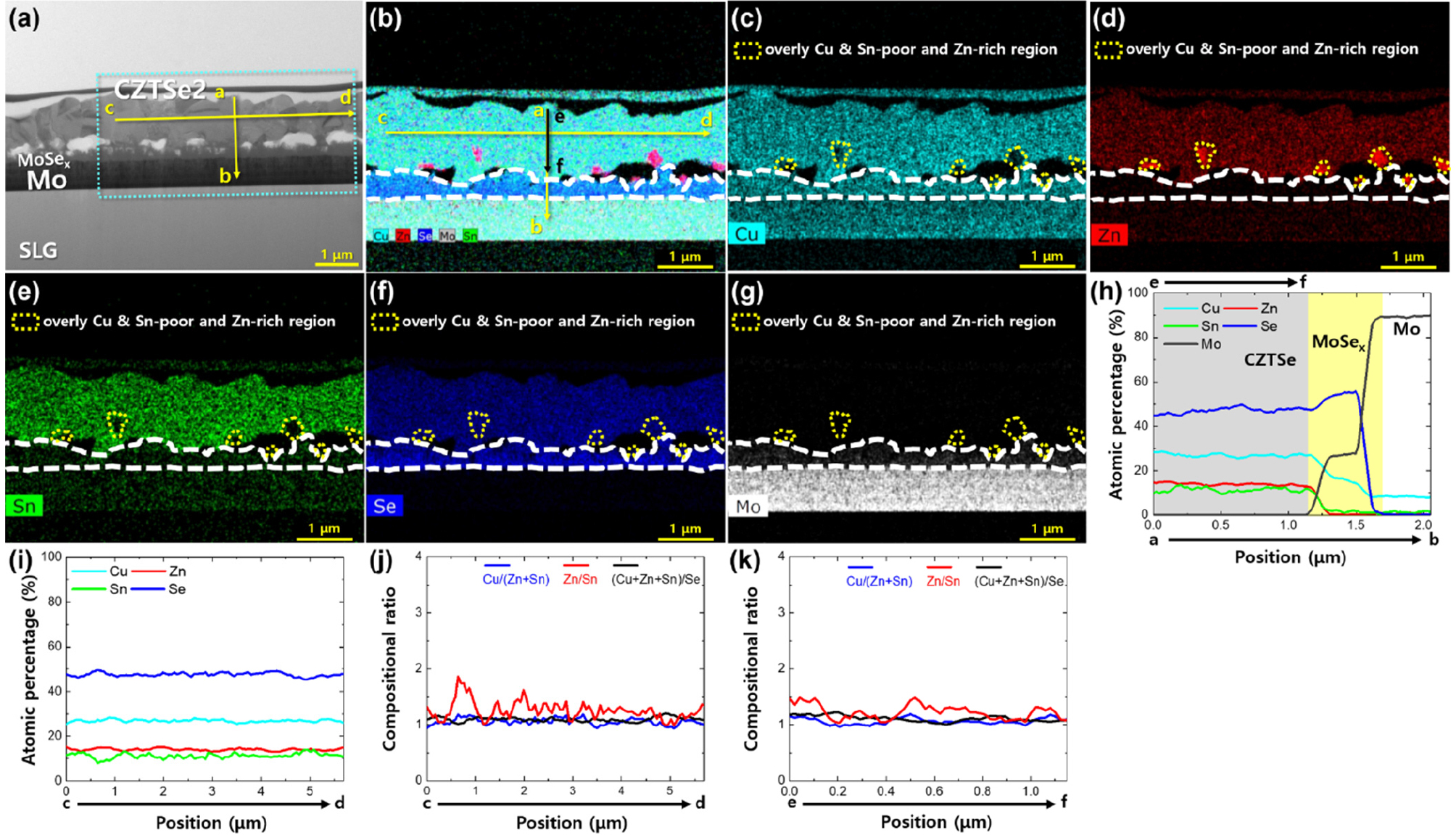
Fig. 4
STEM-EDS mapping images of CZTSe2 thin-film solar cells. (a) Cross-sectional STEM image. EDS mapping images of the CZTSe2 absorber layer showing mappings of (b) Cu, Zn, Sn, Se, and Mo, (c) Cu, (d) Zn, (e) Sn, (f) Se, and (g) Mo. The elemental variations in the vertical and lateral directions in (a) and (b) were measured using EDS line scans. EDS line scans along (h) a→b and (i) c→d. Compositional ratio variations along (j) c→d and (k) e→f
Similar to CZTSe1 and CZTSe2, voids (Fig. 5 (a)) and secondary phases (Figs. 5 (b)-(g)) are observed at the absorber layer-back contact interface of CZTSe3. Fig. 5 (h) shows the formation of a 0.34 μm-thick MoSe2 layer. As shown in Figs. 5 (i) and (j), in the lateral direction c→d in region ①, the average atomic percentages of Cu, Zn, Sn, and Se are 19.3%, 25.4%, 11.3%, and 47.7%, respectively, and the average compositional ratios of [Cu]/([Zn]+[Sn]), [Zn]/[Sn], and ([Cu]+[Zn]+[Sn])/[Se] are 0.61, 4.23, and 1.03, respectively. In addition, in region ① where the maximum Zn atomic percentage is 44.0%, the atomic percentages of Cu, Sn, and Se are 5.6%, 0.5%, and 49.9%, respectively, and the compositional ratios of [Cu]/([Zn]+[Sn]), [Zn]/[Sn], and ([Cu]+[Zn]+[Sn])/[Se] are 0.13, 88.00, and 1.00, respectively. In the lateral direction c→d in the CZTSe3 absorber excluding region ①, the average atomic percentages of Cu, Zn, Sn, and Se are 26.5%, 14.3%, 11.2%, and 48.0%, respectively, and the average compositional ratios of [Cu]/([Zn]+[Sn]), [Zn]/[Sn], and ([Cu]+[Zn]+[Sn])/[Se] are 1.04, 1.28, and 1.08, respectively. Hence, the average compositional ratios in the lateral direction c→d excluding region ① show characteristics similar to those of CZTSe1 and CZTSe2. However, in region ①, the Zn composition increases and the Cu and Sn compositions decrease compared to the average composition in regions other than region ①. Therefore, region ① in the CZTSe3 absorber layer has overly Cu-poor, Sn-poor, and Zn-rich phases. These overly Cu-poor, Sn-poor, and Zn-rich phases should exhibit the same characteristics as the secondary phases found in CZTSe1 and CZTSe2. As shown in Fig. 5 (h), in the vertical direction e→f where no secondary phase is observed, the atomic percentages of Cu, Zn, Sn, and Se are 26.3%, 13.8%, 10.3%, and 49.6%, respectively. Fig. 5 (k) shows average compositional ratios of 1.09, 1.34, and 1.02 for [Cu]/([Zn]+[Sn]), [Zn]/[Sn], and ([Cu]+[Zn]+[Sn])/[Se], respectively. Therefore, compared to the average composition in the lateral direction c→d excluding region ①, the Zn and Sn compositions in the vertical direction e→f decrease.
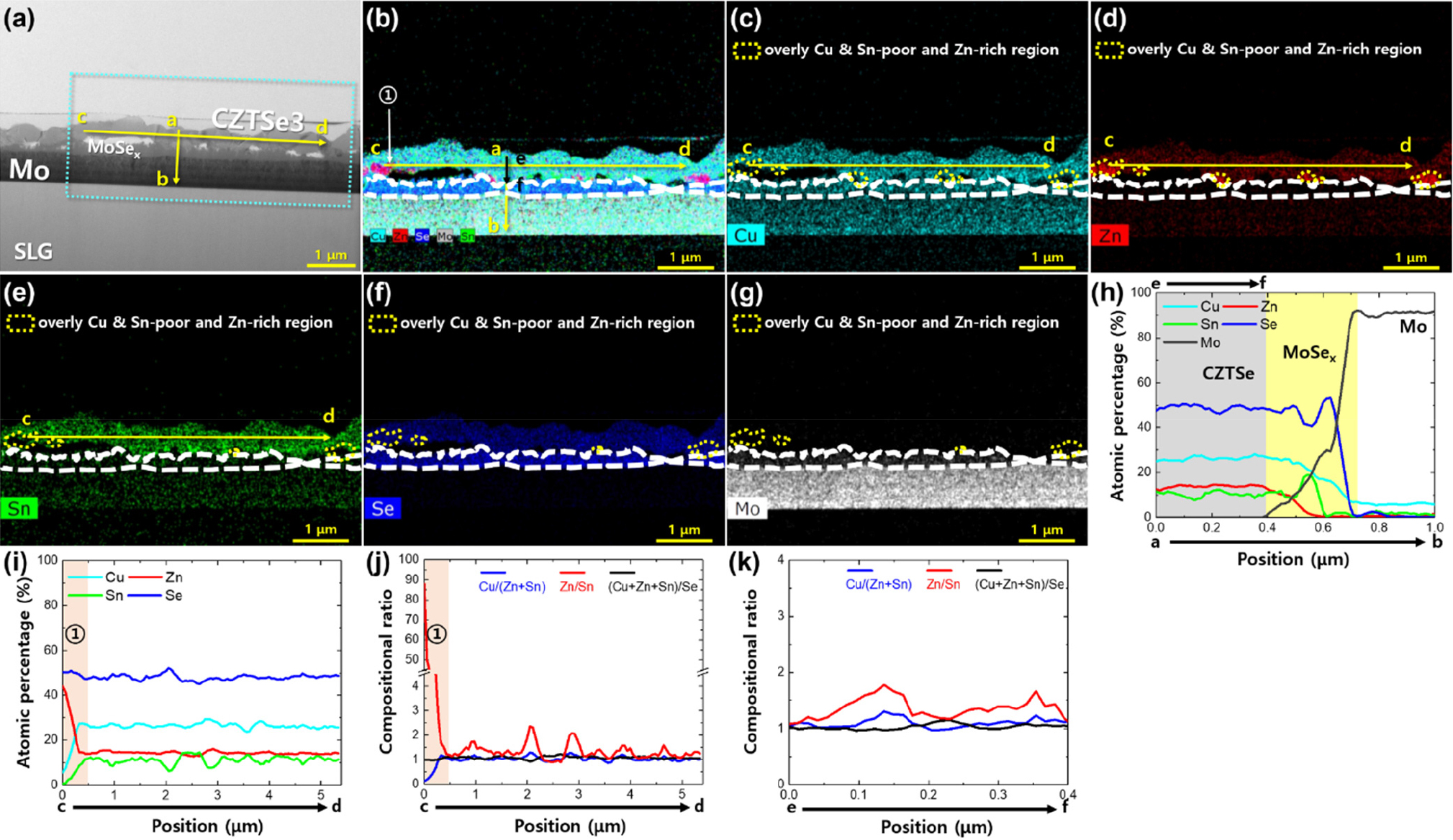
Fig. 5
STEM-EDS mapping images of CZTSe3 thin-film solar cells. (a) Cross-sectional STEM image. EDS mapping images of the CZTSe3 absorber layer showing mappings of (b) Cu, Zn, Sn, Se, and Mo, (c) Cu, (d) Zn, (e) Sn, (f) Se, and (g) Mo. The elemental variations in the vertical and lateral directions in (a) and (b) were measured using EDS line scans. EDS line scans along (h) a→b and (i) c→d. Compositional ratio variations along (j) c→d and (k) e→f
Similar to CZTSe1, CZTSe2, and CZTSe3, voids (Fig. 6 (a)) and secondary phases (Figs. 6 (b)-(g)) are observed at the absorber layer-back contact interface of CZTSe4. In addition, as shown in Fig. 6 (h), the formation of a 0.28 μm-thick MoSe2 layer is observed. As shown in Figs. 6 (i) and (j), in the lateral direction c→d in region ①, the average atomic percentages of Cu, Zn, Sn, and Se are 11.7%, 38.3%, 3.6%, and 46.4%, respectively, and the average compositional ratios of [Cu]/([Zn]+[Sn]), [Zn]/[Sn], and ([Cu]+[Zn]+[Sn])/[Se] are 0.28, 10.64, and 1.16, respectively. In region ① where the maximum Zn atomic percentage is 46.2%, the atomic percentages of Cu, Sn, and Se are 6.7%, 0.3%, and 46.8%, respectively, and the compositional ratios of [Cu]/([Zn]+[Sn]), [Zn]/[Sn], and ([Cu]+[Zn]+[Sn])/[Se] are shown to be 0.14, 154.00, and 1.14, respectively. In the lateral direction c→d in region ② of the CZTSe4 absorber, the average atomic percentages for Cu, Zn, Sn, and Se are 12.0%, 37.4%, 3.1%, and 47.5%, respectively, and the average compositional ratios of [Cu]/([Zn]+[Sn]), [Zn]/[Sn], and ([Cu]+[Zn]+[Sn])/[Se] are 0.30, 12.06, and 1.11, respectively. In addition, in region ② where the maximum Zn atomic percentage is 45.3%, the atomic percentages of Cu, Sn, and Se are 7.3%, 0.7%, and 46.7%, respectively, and the compositional ratios of [Cu]/([Zn]+[Sn]), [Zn]/[Sn], and ([Cu]+[Zn]+[Sn])/[Se] are shown to be 0.16, 64.47, and 1.14, respectively. In the lateral direction c→d in region ③, the average atomic percentages of Cu, Zn, Sn, and Se are 17.6%, 30.3%, 7.3%, and 44.8%, respectively, and the average compositional ratios of [Cu]/([Zn]+[Sn]), [Zn]/[Sn], and ([Cu]+[Zn]+[Sn])/[Se] are 0.47, 4.15, and 1.23, respectively. In region ③ where the maximum Zn atomic percentage is 42.4%, the atomic percentages of Cu, Sn, and Se are 9.8%, 3.7%, and 44.1%, respectively, and the compositional ratios of [Cu]/([Zn]+[Sn]), [Zn]/[Sn], and ([Cu]+[Zn]+[Sn])/[Se] are observed to be 0.21, 11.46, and 1.27, respectively. In the lateral direction c→d in region ④, the average atomic percentages of Cu, Zn, Sn, and Se are 15.0%, 35.1%, 4.1%, and 45.8%, respectively, and the average compositional ratios of [Cu]/([Zn]+[Sn]), [Zn]/[Sn], and ([Cu]+[Zn]+[Sn])/[Se] are 0.38, 8.56, and 1.18, respectively. The maximum Zn atomic percentage in region ④ is 46.3%, with Cu, Sn, and Se atomic percentages of 7.6%, 0.8%, and 45.3%, respectively, and the compositional ratios of [Cu]/([Zn]+[Sn]), [Zn]/[Sn], and ([Cu]+[Zn]+[Sn])/[Se] are 0.16, 57.88, and 1.21, respectively. In the lateral direction c→d in the CZTSe4 absorber excluding regions ①-④, the average atomic percentages of Cu, Zn, Sn, and Se are 28.2%, 14.3%, 11.0%, and 46.5%, respectively, and the average compositional ratios of [Cu]/([Zn]+[Sn]), [Zn]/[Sn], and ([Cu]+[Zn]+[Sn])/[Se] are 1.11, 1.30, and 1.15, respectively. Accordingly, the average compositional ratios in the lateral direction c→d in the CZTSe4 absorber excluding regions ①-④ show similar characteristics to those in CZTSe1, CZTSe2, and CZTSe3. However, in regions ①-④ in the lateral direction c→d in the CZTSe4 absorber, the Zn composition increases and the Cu and Sn compositions decrease compared to the average composition in the region excluding regions ①-④. This indicates that regions ①-④ are overly Cu-poor, Sn-poor, and Zn-rich phases, similar to the secondary phase found in the CZTSe3 absorber layer. As shown in Figs. 6 (h) and (k), in the vertical direction e→f in region ① of the CZTSe4 absorber, the average atomic percentages of Cu, Zn, Sn, and Se are 15.1%, 29.4%, 5.6%, and 49.9%, respectively, and the average compositional ratios of [Cu]/([Zn]+[Sn]), [Zn]/[Sn], and ([Cu]+[Zn]+[Sn])/[Se] are 0.43, 5.25, and 1.00, respectively. In region ① where the maximum Zn atomic percentage is 44.7%, the atomic percentages of Cu, Sn, and Se are 7.5%, 2.2%, and 45.6%, respectively, and the compositional ratios of [Cu]/([Zn]+[Sn]), [Zn]/[Sn], and ([Cu]+[Zn]+[Sn])/[Se] are 0.16, 20.32, and 1.19, respectively. As shown in Figs. 6 (h) and (k), in the vertical direction e→f excluding region ①, the atomic percentages of Cu, Zn, Sn, and Se are 27.9%, 14.2%, 9.1%, and 48.8%, respectively, and the average compositional ratios of [Cu]/([Zn]+[Sn]), [Zn]/[Sn], and ([Cu]+[Zn]+[Sn])/[Se] are 1.20, 1.56, and 1.05, respectively. Therefore, a slight decrease in the Sn composition in the vertical direction e→f excluding region ① is observed compared to the average composition in the lateral direction c→d excluding regions ①-④.
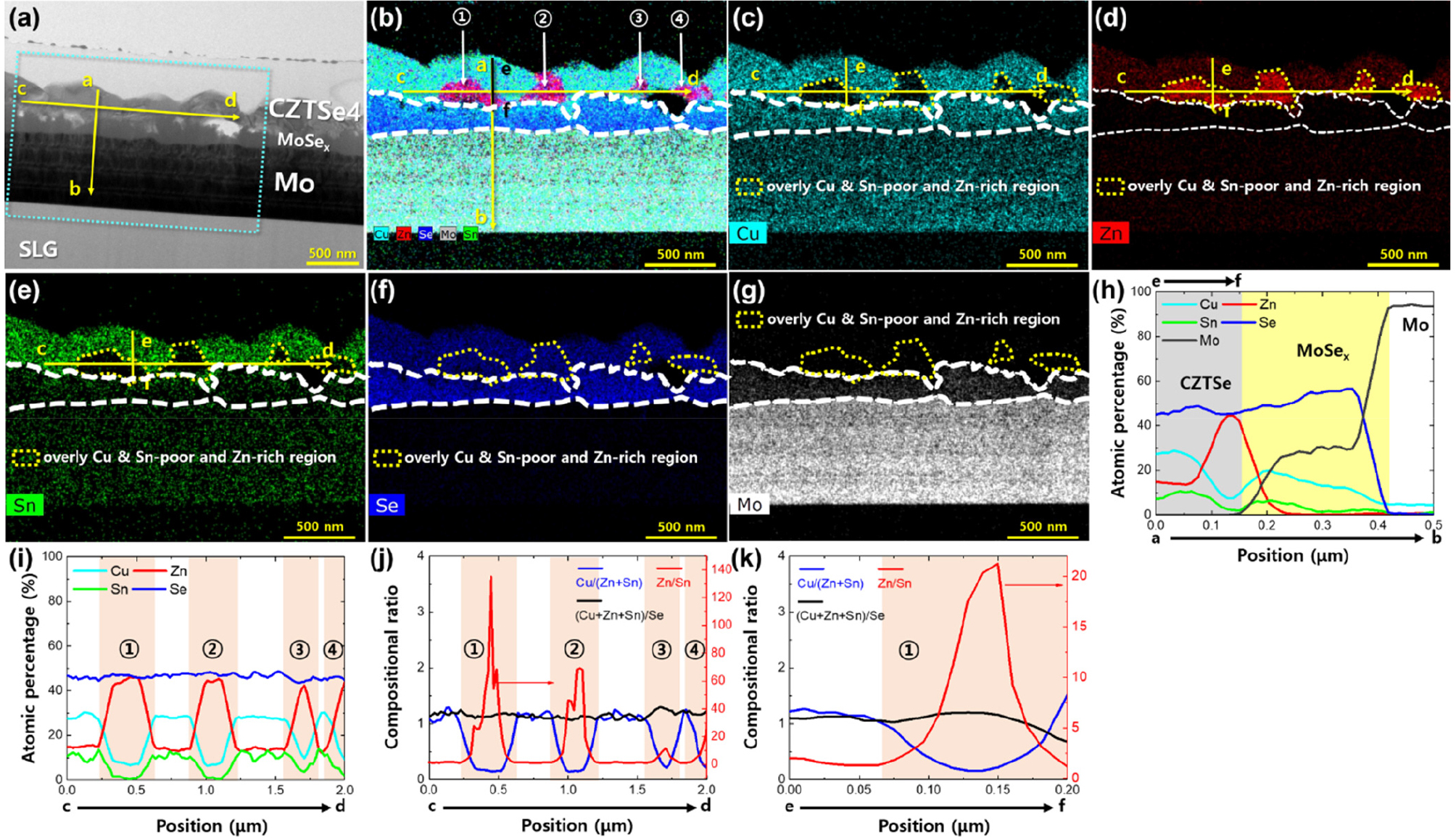
Fig. 6
STEM-EDS mapping images of CZTSe4 thin-film solar cells. (a) Cross-sectional STEM image. EDS mapping images of the CZTSe4 absorber layer showing mappings of (b) Cu, Zn, Sn, Se, and Mo, (c) Cu, (d) Zn, (e) Sn, (f) Se, and (g) Mo. The elemental variations in the vertical and lateral directions in (a) and (b) were measured using EDS line scans. EDS line scans along (h) a→b and (i) c→d. Compositional ratio variations along (j) c→d and (k) e→f
Similar to CZTSe1 - CZTSe4, voids (Fig. 7 (a)) and secondary phases (Figs. 7 (b)-(g)) are observed at the absorber layer-back contact interface of CZTSe5. Fig. 7 (h) illustrates the formation of a 0.23 μm-thick MoSe2 layer. As shown in Figs. 7 (i) and (j), the average atomic percentages of Cu, Zn, Sn, and Se are 22.6%, 20.3%, 8.9%, and 48.2%, respectively, in the lateral direction c→d in region ① of the CZTSe5 absorber. Furthermore, the average compositional ratios of [Cu]/([Zn]+[Sn]), [Zn]/[Sn], and ([Cu]+[Zn]+[Sn])/[Se] are 0.77, 2.28, and 1.07, respectively. In region ① where the maximum Zn atomic percentage is 33.1%, the atomic percentages of Cu, Sn, and Se are observed to be 16.3%, 5.7%, and 44.9%, respectively, and the compositional ratios of [Cu]/([Zn]+[Sn]), [Zn]/[Sn], and ([Cu]+[Zn]+[Sn])/[Se] are shown to be 0.42, 5.81, and 1.23, respectively. In the lateral direction c→d in region ② of the CZTSe5 absorber, the average atomic percentages of Cu, Zn, Sn, and Se are shown to be 16.2%, 30.3%, 5.2%, and 48.3%, respectively. Furthermore, the average compositional ratios of [Cu]/([Zn]+[Sn]), [Zn]/[Sn], and ([Cu]+[Zn]+[Sn])/[Se] are found to be 0.46, 5.83, and 1.07, respectively. In addition, in region ② where the maximum Zn atomic percentage is 40.4%, the atomic percentages of Cu, Sn, and Se are observed to be 10.9%, 1.6%, and 47.1%, respectively, and the compositional ratios of [Cu]/([Zn]+[Sn]), [Zn]/[Sn], and ([Cu]+[Zn]+[Sn])/[Se] are 0.26, 25.25, and 1.12, respectively. In the lateral direction c→d in region ③ of the CZTSe5 absorber, the average atomic percentages of Cu, Zn, Sn, and Se are 26.0%, 18.0%, 8.7%, and 47.3%, respectively, and the average compositional ratios of [Cu]/([Zn]+[Sn]), [Zn]/[Sn], and ([Cu]+[Zn]+[Sn])/[Se] are 0.97, 2.07, and 1.11, respectively. In addition, in region ③ where the maximum Zn atomic percentage is 21.3%, the atomic percentages of Cu, Sn, and Se are observed to be 25.2%, 6.6%, and 46.9%, respectively, and the compositional ratios of [Cu]/([Zn]+[Sn]), [Zn]/[Sn], and ([Cu]+[Zn]+[Sn])/[Se] are calculated as 0.90, 3.23, and 1.13, respectively. In the lateral direction c→d in the CZTSe5 absorber excluding regions ①-③, the average atomic percentages of Cu, Zn, Sn, and Se are 26.3%, 14.4%, 11.5%, and 47.8%, respectively, and the average compositional ratios of [Cu]/([Zn]+[Sn]), [Zn]/[Sn], and ([Cu]+[Zn]+[Sn])/[Se] are 1.02, 1.25, and 1.09, respectively. Accordingly, the average compositions in the lateral direction c→d in the CZTSe5 absorber excluding regions ①-③ show characteristics similar to those in CZTSe1 - CZTSe4. However, in regions ①-③ in the lateral direction c→d in the CZTSe5 absorber, the Zn composition increases and the Cu and Sn compositions decrease compared to the average composition in the region excluding regions ①-③. This implies the formation of overly Cu-poor, Sn-poor, and Zn-rich regions, similar to the secondary phase of the CZTSe3 and CZTSe4 absorber layers. As shown in Figs. 7 (h) and (k), in the vertical direction e→f, the average atomic percentages of Cu, Zn, Sn, and Se are 26.2%, 13.1%, 12.8%, and 47.9%, respectively, and the average compositional ratios of [Cu]/([Zn]+[Sn]), [Zn]/[Sn], and ([Cu]+[Zn]+[Sn])/[Se] are 1.01, 1.02, and 1.09, respectively. This shows that the average compositional ratio [Zn]/[Sn] decreases slightly in the vertical direction e→f compared to that in the lateral direction c→d excluding regions ①-③.
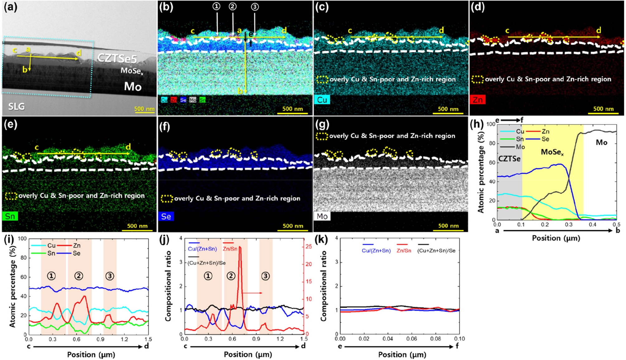
Fig. 7
STEM-EDS mapping images of CZTSe5 thin-film solar cells. (a) Cross-sectional STEM image. EDS mapping images of the CZTSe5 absorber layer showing mappings of (b) Cu, Zn, Sn, Se, and Mo, (c) Cu, (d) Zn, (e) Sn, (f) Se, and (g) Mo. The elemental variations in the vertical and lateral directions in (a) and (b) were measured using EDS line scans. EDS line scans along (h) a→b and (i) c→d. Compositional ratio variations along (j) c→d and (k) e→f
As shown in Figs. 3 - 7, a secondary phase of the CZTSe absorbers containing Cu, Zn, and Sn metal precursors was formed at the CZTSe absorber-Mo back contact interface41, 42). The secondary phase of all samples was overly Cu-poor, Sn-poor, and Zn-rich, and the values of ([Cu]+[Zn]+[Sn])/[Se] ranged from 1.00 to 1.27. This indicates that the value of [Cu]+[Zn]+[Sn] is constant to a certain degree. As shown in Fig. 5 (i), Fig. 6 (i), and Fig. 7 (i), the secondary phase with regions exhibiting overly Cu-poor, Sn-poor, and Zn-rich characteristics can include a ZnSe phase, where AB antisites (A replacing B) and VA (A vacancy) may be generated within the CZTSe crystal structure9, 38). In particular, the overly Cu-poor, Sn-poor, and Zn-rich regions have a low probability of forming VZn, CuZn, SnZn, CuSn, and SnCu, a high probability of forming VCu, VSn, ZnCu, and ZnSn, and a high probability of forming VCu + ZnCu and ZnSn + 2ZnCu defect clusters9). However, the band edge shift due to defect clusters VCu + ZnCu and ZnSn + 2ZnCu is negligible43). Defect formation is related to the secondary phase, and the defect density directly affects the VOC deficit (Eg/q - VOC)33, 34). Among VCu, VSn, ZnCu, and ZnSn, the defects VCu and ZnCu exhibit relatively shallow defect levels and are not considered detrimental. At various acceptor levels, VSn-1, VSn-2, VSn-3, and VSn-4 for VSn and ZnSn-1 and ZnSn-2 for ZnSn, deep defect levels are observed43). Defects in the absorber layer act as electron-hole recombination centers38). From the VOC deficit values in Fig. 2 (h), it was deduced that the defect-related VOC loss is higher in the thinner absorber layers than in the thicker absorber layers. These defects are possibly related to the ZnSe phase in the overly Cu-poor, Sn-poor, and Zn-rich regions. The ZnSe phase observed in Fig. 3 to Fig. 7 reached a size close to the thickness of the absorber layer as the CZTSe thickness decreased. As the CZTSe thickness decreased, the size of the ZnSe phase became relatively large compared to the thickness of the absorber, which can be explained using the principles of thermodynamics. For metal precursors, the reaction mechanism with Se is as follows:36)
In a previous work, the growth of MoSe2 was modeled with a three-step process: diffusion of Se through CZTSe, diffusion through MoSe2 growing with continued annealing and reaction between Se and Mo, and growth of MoSe2 during the high-temperature process of a CZTSe absorber limited by the diffusion of Se through the CZTSe layer44). In this selenization process, the amount of Se pellets is kept constant at 0.65 g. Thus, the partial pressure of Se in the RTP chamber is expected to remain the same. As shown in Fig. 3 to Fig. 7, as the CZTSe thickness decreased, the MoSe2 thickness also decreased to 0.9 μm (CZTSe1), 0.4 μm (CZTSe2), 0.34 μm (CZTSe3), 0.28 μm (CZTSe4), and 0.23 μm (CZTSe5). Since the free energy (ΔG) of reaction (8) is -186 kJ/mol at 550°C and spontaneous reaction predominates45), the decrease in the diffusion of Se through the CZTSe layer can cause a decrease in the MoSe2 thickness according to the decrease in the precursor thickness. This implies that during the selenization process of the precursor, Se consumption increases as the precursor thickness decreases. As the precursor thickness decreases, the amount of Se consumed by reaction (2) decreases, and the Se flux in reactions (4) and (5) increases. In addition, the ΔG of reaction (5) is -304 kJ/mol at 550°C, indicating a spontaneous reaction character45). Therefore, the formation of the ZnSe phase increases. However, from the reaction between ZnSe and Mo, ΔG is 118 kJ/mol at 550°C, which means that the probability of the decomposition of ZnSe and the formation of MoSe2 by the reaction of ZnSe and Mo at the CZTSe absorber-Mo interface is low45). As shown in Figs. 3-7, as the thickness of the precursor decreases, the ratio of the ZnSe phase thickness to the CZTSe layer thickness (ZnSe/CZTSe thickness ratio) increases from 0.21 (CZTSe1) to 0.32 (CZTSe2), 0.51 (CZTSe3), ~1.00 (CZTSe4), and ~1.00 CZTSe5. Thus, the relative increase in the ZnSe phase formed in the CZTSe layer according to the decrease in the precursor thickness can cause VOC loss due to defects, resulting in decreased efficiency.
4. Conclusion
We examined the performance of CZTSe solar cells with various absorber layer thicknesses. We confirmed that both JSC and VOC decrease as the CZTSe absorber thickness decreases. The decrease in JSC with decreasing absorber thickness can be attributed to the small grain size, increased electron-hole recombination at the back contact electrode, and increased reflection at the back contact electrode. The grain size of the CZTSe absorber can be increased through alkali metal doping and temperature control of the heat treatment process. The electron-hole recombination and reflection at the back contact can be improved through Eg engineering and back contact passivation of the CZTSe absorber bottom layer. In addition, the decrease in VOC with decreasing absorber thickness can be attributed to the change in the ratio of the ZnSe phase thickness to the CZTSe layer thickness. These ZnSe phases can result in various defects and defect clusters. The formation of the ZnSe phase as the CZTSe absorber thickness decreases can be suppressed by controlling the Se partial pressure during the selenization process. Thus, to realize high-efficiency ultrathin CZTSe-based solar cells, uniform composition distribution for the suppression of ZnSe formation in the absorber layer, bandgap engineering, and back contact passivation of the CZTSe absorber bottom layer are important.
