Nomenclature
Isc : short circuit current, A
Jsc : short circuit current density, mA/cm2
Voc : open circuit voltage, V
FF : Fill factor, %
Eff : efficiency, %
Subscript
TOPCon : Tunnel oxide passivated contact
PERC : Passivated emitter and rear cell
SHJ : Silicon Heterojunction cell
PV: Photovoltaics
SiNx : Silicon nitride
ARC : Anti reflection coating
PL : Photoluminescence
Ag : Silver
Al : Aluminum
LECO : Laser Enhanced Contact Optimization
1. 서 론
스크린 인쇄 기법은 금속 페이스트를 메쉬 기판에 스퀴즈를 통해 압착함으로서 다양한 기판에 원하는 패턴을 구현할 수 있는 전극 형성 기법이다1). 스크린 인쇄 기법은 결정질 실리콘 태양전지 공정 중 산업 규모의 전극 형성을 위한 주요 방법으로 발전해 왔다. 오늘날 전 세계 결정질 실리콘 태양 전지의 98% 이상이 스크린 인쇄를 사용하여 전극이 형성된다2). 지난 수십 년간 스크린 인쇄가 주요 전극 형성 기법으로 채택된 것은 다른 전극 형성 기법에 비해 높은 생산성과 비용 효율성, 높은 신뢰성에서 기인한다. 때문에 전세계 PV 시장에서 가장 큰 비중을 가진 p-type PERC (Passivated Emitter and rear cell), n-type TOPCon (Tunnel Oxide Passivated Contact) 구조의 태양전지의 전,후면전극 형성에 스크린 인쇄 공정이 채택되고 있다3,4). 결정질 실리콘 태양전지의 Ag 전면 전극은 셀의 저항, FF (Fill factor), 제조단가 등의 요소에 많은 영향을 미치기 때문에 PV 분야의 발전단가 하락을 위해 셀의 효율을 높이면서 단가를 낮추는 방향으로 기술 개발이 진행되었다5). 태양전지의 Ag 소모량 절감과 고효율화를 동시에 달성하기 위해, 전극의 선폭을 낮춰 수광 면적을 늘려 셀의 FF를 향상시킴과 동시에 생산단가의 많은 부분을 차지하는 Ag 페이스트의 사용량을 줄이는 방향으로 연구가 진행되고 있다2)(Fig. 1).
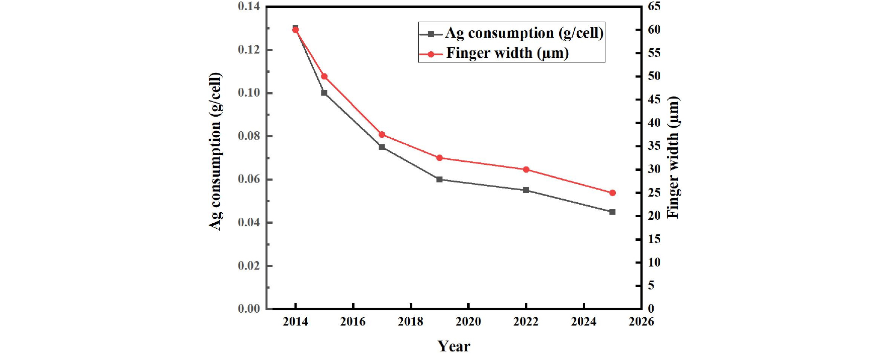
Fig. 1
Predicted trend for finger width and Ag consumption2-6)
이는 전극의 소성 공정 시에 일어나는 전극과 셀 간의 계면반응에 대한 최적화가 진행되어 높은 면저항을 가지는 Si 웨이퍼에 낮은 접촉저항을 갖는 Ag 페이스트의 사용이 가능해졌기 때문이다7). 본론에서는 결정질 실리콘 태양전지에 적용되는 스크린 인쇄 관련 연구 동향을 인쇄 공정, 소성 공정, 공정 중 분석기술, TOPCon 및 SHJ (Silicon Heterojunction cell)에 대한 스크린 인쇄 공정의 영향 순으로 기술한다.
2. 본 론
2.1 스크린 인쇄 공정
지난 수년간 Ag paste 기술의 발전 외에도 스크린 인쇄 기술 측면에서 지속적인 발전이 있었다. 전면 전극 선폭의 감소에는 금속 페이스트의 점도 개선, 실리콘 웨이퍼 텍스쳐링 피라미드의 크기 감소8), 메쉬 스크린 제작 기술 발전 등의 요인이 작용했다. 통상적으로 450×450 mm2 크기의 스크린에 들어가는 와이어의 개수, 직경 별로 스크린을 구분하며, 360, 440 mesh보다 더 촘촘한 530 메쉬 스크린을 이용하여 20 μm 선폭을 달성한 케이스가 보고되었다6)(Fig. 2).
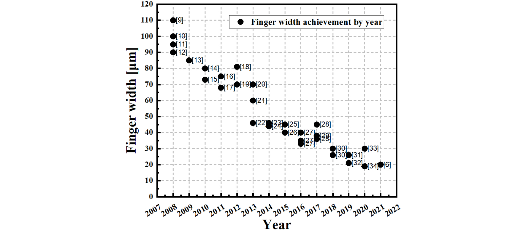
Fig. 2
Cases of finger width reduction in 2008-20219-34)
선폭이 좁아질수록 저항성 손실이 증가하지만, Ag 소모량 감소 및 수광 면적의 증가로 인하여 저항성 손실을 상회하는 경제적, 광학적 이점을 얻을 수 있다35). 선폭과 재료비 절감 외에도 스크린 인쇄 공정 자체의 생산량을 높여 제조원가를 낮추려는 방향의 연구도 진행되고 있다. 일반적인 스크린 인쇄 장비에서는 페이스트를 기판에서 밀어내는 스퀴즈와 밀려난 금속 페이스트를 다시 스크린에 도포하는 스크래퍼가 장착되어있다. 기존 공정은 스퀴즈가 횡방향으로 동작하여 인쇄한 후 다시 스크래퍼가 스퀴즈의 반대방향으로 동작하여 금속 페이스트를 제판에 도포하는 과정을 거치나, 인쇄와 동시에 페이스트를 도포하도록 하여 같은 시간 동안 2번 인쇄가 가능한 인쇄 과정이 제시되었으며, 이를 통해 7,500 wafer/hour의 처리량을 얻을 수 있다36).
2.2 스크린 인쇄 후 소성 기술
인쇄 후 단계, 즉 고온에서의 전극 소성도 태양전지 성능에 매우 중요하다. SiNx ARC를 통한 스크린 인쇄 Ag paste의 소성을 통한 접촉 형성은 복잡한 화학적, 물리적 과정으로, 페이스트 내의 glass frit이 녹고, SiNx가 식각되고, glass frit에 Ag가 용해되며, 실리콘-glass frit 계면에 Ag 결정체가 형성되며, 최종 구조가 형성된다. 일련의 과정이 단 몇 초 간의 융해 및 냉각에 의해 결정되므로, 접촉점에서 낮은 저항과 재결합 손실을 달성하려면 firing step 동안의 태양전지 표면의 정확한 온도를 측정하여 페이스트의 특성에 맞는 온도를 찾는 것이 중요하다37). 연속적인 소성로를 통해 벨트 상에서 셀을 이송하는 공정 단계가 잘 확립되어 있지만, 원하는 온도 프로파일을 유지하면서 벨트 속도를 증가시켜 처리량을 높이고, 인라인 적외선 서모그래피를 이용한 소성로 모니터링38,39)을 도입하여 전극과 emitter 간의 접촉 특성을 더욱 개선할 수 있다. 또한 소성 공정중 LECO (Laser enhanced contact optimization)공정을 적용하면 셀의 금속-반도체 간 접촉 특성을 개선하여 접촉저항을 낮출 수 있다40). 태양 전지 생산 라인 내 셀 불량의 원인은 대부분 금속과 반도체 간의 불완전한 접촉으로 발생한다. 불량 접촉 셀에 LECO 처리를 통해 국소적인 Ag-Si 간 접촉을 형성하도록 하여 생산 기준에 부합하도록 개선하거나, LECO 전용 페이스트를 사용하여 광전환 효율을 높인 사례가 보고되었다41).
2.3 스크린 인쇄 공정 분석 기술
결정질 실리콘 태양전지의 전기적 성능을 최대로 달성하기 위해서는 최소한의 접촉저항으로 emitter와 금속 전극 사이에 ohmic contact을 이루는 것이 중요하다42). 높은 종횡비로 균일하면서 결점 없는 전극 형상을 달성하기 위해서는 스크린 인쇄 프로세스의 물리적인 동작에 대한 이해가 필요하다. 이를 위해 밀리초 단위로 촬영이 가능한 카메라를 사용하여 스크린 인쇄 공정 중 금속 페이스트가 스크린, 인쇄기판, 스크린의 개구부 사이에서 어떠한 물리적, 기계적 거동을 보이는지 분석하는 비디오 이미지 분석 기술이 연구되었다43).
2.4 TOPCon cell에 스크린 인쇄가 미치는 영향
n-TOPCon 구조에서 Boron emitter는 터널 SiO2층에 의해 금속 전극과 분리된다. 이때 각 층의 적층 상태 및 소성 매개변수가 접촉저항과 캐리어의 재결합에 미치는 영향을 분석하여 낮은 재결합과 접촉저항을 동시에 달성할 수 있는 조건이 발견되었다44,45).
2.5 저온 소성 Ag paste에 적용되는 스크린 인쇄 공정
n-type SHJ에 적용되는 저온 소성 Ag paste는 인쇄되는 그리드 구조의 품질을 높이기 위해 인쇄 속도가 200 mm/s로 제한된다. 스크린 인쇄 공정의 낮은 속도로 인하여 셀의 공정 처리량도 상대적으로 낮아지며 이는 PERC의 백엔드 라인의 셀 처리량의 40%에 해당한다. 이때 스크린 인쇄 후 건조 및 경화 공정 중 IR radiation을 추가로 가함으로써 경화시간을 줄이고 광흡입 효과를 증가시켜 높은 처리량 및 기존 대비 개선된 표면 패시베이션 특성을 얻을 수 있다46).
3. 결 론
Ag, Al paste를 이용한 스크린 인쇄 공정은 결정질 실리콘 태양전지의 성능과 제조비용에 큰 영향을 미친다. 현재 상업용 결정질 실리콘 태양전지의 98% 이상이 스크린 인쇄 방법에 의해 제조되고 있다. 태양전지의 제조단가를 낮추기 위해, 기존 보다 더욱 좁은 선폭을 안정적으로 형성하는 530 mesh screen 기반 인쇄 기술이 소개되었다. 스크린 프린터에 물리적으로 고해상력의 카메라를 설치하여 인쇄 순간의 금속 페이스트의 물리적 거동이 설명되었으며, n-type TOPCon 구조의 터널 층에 전극의 소성 공정이 미치는 영향 등이 분석되었으며, SHJ에 적용되는 저온소성 페이스트에 대한 처리량 개선 방안이 소개되었다. 스크린 인쇄 기술의 기술 발전 동향을 종합해보면, 향후 전극 형성 공정에서는 Ag의 소모를 줄이고, 생산 속도, 즉 시간당 셀 처리량을 증가시켜 저비용 고효율화를 달성할 것으로 예상된다.
Acknowledgements
본 연구는 2019년도 정부(산업통상자원부)의 재원으로 한국에너지기술평가원의 지원을 받아 수행된 연구(20193020010650, 인쇄 한계 극복을 위한 전극형성/모듈 일체화 기술 개발)일환으로 수행되었습니다.
이 논문은 2021~2022년도 청주대학교 연구장학 지원에 의한 것임.
References
Danjela Kuscer, "Screen Printing," Encyclopedia of Materials: Technical Ceramics and Glasses, 1, 227-232 (2021).
10.1016/B978-0-12-803581-8.12082-XITRPV, International Technology Roadmap for Photovoltaic (ITRPV): Results 2021, (twelfth ed.), 13-24 (2021).
Chen Daming et al., "24.58% total area efficiency of screen-printed, large area industrial silicon solar cells with the tunnel oxide passivated contacts (i-TOPCon) design," Solar Energy Materials and Solar Cells, 206, 110258 (2020).
10.1016/j.solmat.2019.110258W. Deng et al., "22.61 % Efficient Fully Screen Printed PERC Solar Cell," 2017 IEEE 44th Photovoltaic Specialist Conference (PVSC), 2220-2226 (2017).
10.1109/PVSC.2017.8366416조성빈, 김희수, 허주열, "결정질 실리콘 태양전지 전면전극 형성기술 개발 동향," 한국태양광발전학회지, 1(2), 15-27 (2015).
Wenzel Timo et al., "Progress with screen printed metallization of silicon solar cells - Towards 20 μm line width and 20 mg silver laydown for PERC front side contacts," Solar Energy Materials and Solar Cells, 244, 111804 (2022).
10.1016/j.solmat.2022.111804Hilali, M. M., "Understanding and development of manufacturable screen -printed contacts on high sheet-resistance emitters for low -cost silicon solar cells," Available from ProQuest Dissertations & Theses Global. (304999350) (2005).
M. Aoki and I. Sumita, "Requirements of Screen masks for Fine-line Printing on Textured Surface," Poster presentation at 8th Workshop on Metallization and Interconnection for Crystalline Silicon Solar Cells (2019).
A. Mette, "Potential of both sides contacted solar cells," Presented on Crystal Clear Workshop on Metallization, 10 (2008).
M. Horteis, "Aerosol-printed silicon solar cell exceeding 20% efficiency," Presented on Crystal Clear Workshop on Metallization, 10 (2008).
D. Erath, "Advanced screen printing technique for high definition front side metallization of crystalline silicion solar cells," Presented on Crystal Clear Workshop on Metallization, 10 (2008).
M. Hofmann, D. Erath, B. Bitnar, L. Gautero, J. Nekarda, A. Grobe, D. Biro, J. Rentsch, R. Preu, "Industrial type Cz Silicon Cells with screen-printed fine line front contacts and passivated rear contacted by laser firing," Proc. Of the 23rd Photovoltaic Solar Energy Conference (EUPVSEC), 1-5 (2008).
F. Clement, "Die Metal Wrap Through Solarzelle: Entwicklung und Charakterisierung," Dissertation, Freiburg (2009).
T. Falcon, A. Hobby, "High accuracy, high aspect ratio metallization on silicon solar cells using a print on print process," Proc. Of the 25th Photovoltaic Solar Energy Conference (EUPVSEC), 1651-1655 (2010).
M. Galiazzo, V. Furin, D. Tonini, G. Cellere, A. Baccini, "Double printing of front contact Ag in c-Si solar cells," Proc. Of the 25th Photovoltaic Solar Energy Conference (EUPVSEC), 2338-2340 (2010).
P. Magnone, R. de Rose, M. Zanuccoli, D. Tonini, M. Galiazzo, G. Cellere, H.- W. Guo, M. Frei, E. Sangiorgi, C. Fiegna, "Understanding the impact of double screen-printing on silicon solar cells by 2-D numerical simulations," Conference Records of the 37th IEEE Photovoltaic Specialists Conference (PVSC), 2177-2180 (2011).
10.1109/PVSC.2011.6186388H. Hannebauer, T. Falcon, R. Hesse, T. Dullweber, R. Brendel, "18,9%-efficient screen-printed solar cells applying a print-on-print process," Proc. Of the 26th Photovoltaic Solar Energy Conference (EUPVSEC), 1607-1610 (2011).
M. Pesce, M. Maugeri, M. Marsili, M. Zarcone, D. Tonini, C. Bottosso, M. Galiazzo, A. Tomasi, "Technological and economic assessment of two-steps printing processes in a mc-Si solar cells production environment," Energy Proc. 21, 24-31 (2012).
10.1016/j.egypro.2012.05.004T. Dullweber, S. Gatz, H. Hannebauer, T. Falcon, R. Hesse, J. Schmidt, R. Brendel, "Towards 20% efficient large-area screen-printed rear-passivated silicon solar cells," Prog. Photovoltaics Res. Appl. 20, 630-638 (2012).
10.1002/pip.1198A.F. Carroll, "Screen printed metal contacts to Si solar cells - formation and synergistic improvements," Conference Records of 39th IEEE Photovoltaic Specialists Conference (PVSC), 3435-3440 (2013).
10.1109/PVSC.2013.6745186H. Hannebauer, T. Dullweber, T. Falcon, X. Chen, R. Brendel, "Record low Ag paste consumption of 67.7 mg with dual print," Energy Proc. 43, 66-71 (2013).
10.1016/j.egypro.2013.11.089Y.-H. Chang, W.-M. Su, P.-S. Huang, L.-W. Cheng, "Improvement of the solar cell efficiency by fine line print on print technology," Conference Records of 39th IEEE Photovoltaic Specialists Conference (PVSC), 2176-2178 (2013).
10.1109/PVSC.2013.674490623714323H. Hannebauer, T. Dullweber, U. Baumann, T. Falcon, R. Brendel, "21.2%-efficient fineline-printed PERC solar cell with 5 busbar front grid," Phys. Status Solidi Rapid Res. Lett., 675-679 (2014).
10.1002/pssr.201409190M. Galiazzo, A. Voltan, E. Bortoletto, M. Zamuner, M. Martire, O. Borsato, M. Bertazzo, D. Tonini, "Fine line double printing and advanced process control for cell manufacturing," Energy Proc. 67, 116-125 (2015).
10.1016/j.egypro.2015.03.295A. Voltan, M. Galiazzo, F. Oberholtzer, M. Emsley, C.E. Dube, J.G. Graff, "Cell efficiency improvement of fully implanted nPERT solar cells realized through metallization optimization," Proc. of the 31st Photovoltaic Solar Energy Conference (EUPVSEC), 779-782 (2015).
M. Galiazzo, O. Borsato, E. Bortoletto, "Fine line double printing for today and tomorrow cell metallization and interconnection," Proc. Of the 32nd Photovoltaic Solar Energy Conference (EUPVSEC), 958-960 (2016).
M. Galiazzo, "Status and Perspectives of Metallization Technologies for HVM," Presented on 7th Metallization Workshop, 22-23 (2017).
S. Werner, E. Lohmüller, P. Saint-Cast, J. Greulich, J. Weber, S. Schmidt, A. Moldovan, A. Brand, T. Dannenberg, S. Mack, S. Wasmer, M. Demant, M. Linse, R. Ackermann, A. Wolf, R. Preu, "Key aspects for fabrication of p-type Cz-Si PERC solar cells exceeding 22% conversion efficiency," Proc. Of the 33rd Photovoltaic Solar Energy Conference (EUPVSEC), 25-29 (2017).
A. Lorenz, M. Linse, H. Frintrup, M. Jeitler, A. Mette, M. Lehner, R. Greutmann, H. Brocker, M. Konig, D. Erath, F. Clement, "Screen printed thick film metallization of silicon solar cells - recent developments and future perspectives," Proc. Of the 35th Photovoltaic Solar Energy Conference (EUPVSEC), 819-824 (2018).
F. Clement, M. Linse, S. Tepner, N. Wengenmeyr, L. Ney, K. Krieg, A. Lorenz, M. Pospischil, S. Bechmann, K. Oehrle, S. Steckemetz, R. Preu, "Project FINALE - screen and screen printing process development for ultra-fine-line contacts below 20 μm finger width," Proc. Of the 36th Photovoltaic Solar Energy Conference (EUPVSEC), 9-13 (2019).
S. Tepner, N. Wengenmeyr, L. Ney, M. Linse, M. Pospischil, F. Clement, "Improving wall slip behavior of silver pastes on screen emulsions for fine line screen printing," Sol. Energy Mater. Sol. Cells, 109969 (2019).
10.1016/j.solmat.2019.109969E. Lohmüller, J. Greulich, P. Saint-Cast, S. Lohmmüller, S. Schmidt, U. Belledin, T. Fellmeth, S. Mack, G. Emanuel, K. Krieg, M. Zimmer, R. Kunert, F. Zobel, M. Linse, J. Horzel, M. Meßmer, A. Wolf, R. Preu, "Front side optimization on boron- and gallium-doped Cz-Si PERC solar cells exceeding 22% conversion efficiency," Proc. Of the 37th European Photovoltaic Conference (EUPVSEC), 7-11 (2020).
S. Tepner, L. Ney, M. Linse, A. Lorenz, M. Pospischil, F. Clement, "Studying knotless screen patterns for fine line screen printing of Si solar cells," IEEE Journal of Photovoltaics, 10, 319-325 (2020).
10.1109/JPHOTOV.2019.2959939S. Tepner, L. Ney, M. Linse, A. Lorenz, M. Pospischil, K. Masuri, F. Clement, "Screen pattern simulation for an improved front-side Ag-electrode metallization of Si-solar cells," Prog. Photovoltaics Res. Appl., 1054-1062 (2020).
10.1002/pip.3313B. B. van Aken, S. Ramesh, K. J. J. Tool, J. Loffler, A. Weeber and G. J. M. Janssen, "Optimizing front and rear metallization grids for bifacial annual yield," Poster presentation at 8th Workshop on Metallization and Interconnection for Crystalline Silicon Solar Cells (2019).
M. Galiazzo, "Enabling 7,500 wph Productivity by a Novel Screen Printing Process," Presentation at 8th Workshop on Metallization and Interconnection for Crystalline Silicon Solar Cells (2019).
D. Ourinson, G. Emanuel, A. Csordás, G. Dammaß, H. Müller, C. Sternkiker, F. Clement and S. W. Glunz, "In-situ wafer temperature measurement during firing process via inline infrared thermography," Presentation at 8th Workshop on Metallization and Interconnection for Crystalline Silicon Solar Cells (2019).
10.1063/1.5125878G. Emanuel, D. Ourinson, G. Dammaß, H. Müller, C. Sternkiker, F. Ogiewa, K. Rahmanpour, T. Javaid, A. Csordás, S. Nold, S. W. Glunz and Clement, F., "
Project "FEUERDRACHE": Process Development and Control of Contact Firing Processes for High-Efficiency Silicon Solar Cells," Presentation at 9th Workshop on Metallization and Interconnection for Crystalline Silicon Solar Cells (2020).
10.1063/5.0056036G. Emanuel, D. Ourinson, G. Dammaß, H. Müller, C. Sternkiker, F. Ogiewa, K. Rahmanpour, T. Javaid, A. Csordás, S. Nold, S. W. Glunz and F. Clement, "Project "FEUERDRACHE": Process Development and Control of Contact Firing Processes for High-Efficiency Silicon Solar Cells," These proceedings (2021).
10.1063/5.0056036E. Krassowski, S. Großer, Turek, Marko, Henning, Andreas and H. Zhao, "Investigation of monocrystalline p-type PERC cells featuring the Laser Enhanced Contact Optimization process and new LECO paste," These proceedings (2021).
10.1063/5.0056380E. Krassowski, B. Jaeckel, U. Zeller, M. Pander, P. Schenk, Eckehard Hofmueller, "Reliability Evaluation of Photovoltaic Modules Fabricated from Treated Solar Cells by Laser-Enhanced Contact Optimization Process," Special Issue : EUPVSEC, 6, 2100537 (2022).
10.1002/solr.202100537Yang Yi, Seyedmohammadi Shahram, Kumar Umesh, Gnizak Dave, Graddy E.d. and Shaikh Aziz, "Screen Printable Silver Paste For Silicon Solar Cells With High Sheet Resistance Emitters," Energy Procedia, 8, 607-613 (2011).
10.1016/j.egypro.2011.06.190K. Abdel Aal and N. Willenbacher, "Highspeed Video Analysis of The Paste Transfer Process During Screen Printing," Presentation at 9th Workshop on Metallization and Interconnection for Crystalline Silicon Solar Cells (2020).
J. J. Diaz Leon, C. Allebé, A. Ingenito, F.-J. Haug , M. Despeisse, C. Ballif and S. Nicolay, Lean "Integration of p- and n-type passivating contacts by PECVD and PVD," Presentation at 9th Workshop on Metallization and Interconnection for Crystalline Silicon Solar Cells (2020).
A. Chaudhary, J. Hoß, Jan Lossen, René van Swaaij and M. Zeman, "Advancement in screen printed fire through silver paste metallisation of polysilicon based passivating contacts," Presentation at 9th Workshop on Metallization and Interconnection for Crystalline Silicon Solar Cells (2020).
10.1063/5.0055978D. Erath, S. Pingel, R. Khotimah, A. De Rose, D. Eberlein, T. Wenzel, A. Lorenz and F. Clement, "Fast screen printing and curing process for silicon heterojunction solar cells," Presentation at 9th Workshop on Metallization and Interconnection for Crystalline Silicon Solar Cells (2020).
10.1063/5.0056429

